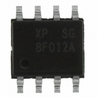
Z8F012ASB020SG Zilog, Z8F012ASB020SG Datasheet - Page 116

Z8F012ASB020SG
Manufacturer Part Number
Z8F012ASB020SG
Description
IC ENCORE XP MCU FLASH 1K 8SOIC
Manufacturer
Zilog
Series
Encore!® XP®r
Datasheet
1.Z8F011ASB020EG.pdf
(282 pages)
Specifications of Z8F012ASB020SG
Core Processor
Z8
Core Size
8-Bit
Speed
20MHz
Connectivity
IrDA, UART/USART
Peripherals
Brown-out Detect/Reset, LED, LVD, POR, PWM, Temp Sensor, WDT
Number Of I /o
6
Program Memory Size
1KB (1K x 8)
Program Memory Type
FLASH
Eeprom Size
16 x 8
Ram Size
256 x 8
Voltage - Supply (vcc/vdd)
2.7 V ~ 3.6 V
Data Converters
A/D 4x10b
Oscillator Type
Internal
Operating Temperature
0°C ~ 70°C
Package / Case
8-SOIC (3.9mm Width)
Processor Series
Z8F012Ax
Core
eZ8
Data Bus Width
8 bit
Data Ram Size
256 B
Interface Type
UART
Maximum Clock Frequency
20 MHz
Number Of Programmable I/os
6
Number Of Timers
2
Operating Supply Voltage
2.7 V to 3.6 V
Maximum Operating Temperature
+ 70 C
Mounting Style
SMD/SMT
Development Tools By Supplier
Z8F04A08100KITG, Z8F04A28100KITG, ZENETSC0100ZACG, ZENETSC0100ZACG, ZUSBOPTSC01ZACG, ZUSBSC00100ZAC, ZUSBSC00100ZACG
Minimum Operating Temperature
0 C
On-chip Adc
10 bit, 4 Channel
Lead Free Status / RoHS Status
Lead free / RoHS Compliant
Other names
269-4039
Z8F012ASB020SG
Z8F012ASB020SG
- Current page: 116 of 282
- Download datasheet (4Mb)
PS022825-0908
DE
1
0
1
0
Idle State
Figure 14. UART Driver Enable Signal Timing (shown with 1 Stop Bit and Parity)
of Line
UART Interrupts
Driver Enable is an active High signal that envelopes the entire transmitted data frame
including parity and Stop bits as displayed in
when a byte is written to the UART Transmit Data register. The Driver Enable signal
asserts at least one UART bit period and no greater than two UART bit periods before the
Start bit is transmitted. This allows a setup time to enable the transceiver. The Driver
Enable signal deasserts one system clock period after the final Stop bit is transmitted. This
one system clock delay allows both time for data to clear the transceiver before disabling
it, as well as the ability to determine if another character follows the current character. In
the event of back to back characters (new data must be written to the Transmit Data Regis-
ter before the previous character is completely transmitted) the DE signal is not deasserted
between characters. The DEPOL bit in the UART Control Register 1 sets the polarity of
the Driver Enable signal.
The Driver Enable to Start bit setup time is calculated as follows:
The UART features separate interrupts for the transmitter and the receiver. In addition,
when the UART primary functionality is disabled, the Baud Rate Generator can also
function as a basic timer with interrupt capability.
Transmitter Interrupts
The transmitter generates a single interrupt when the Transmit Data Register Empty bit
(TDRE) is set to 1. This indicates that the transmitter is ready to accept new data for trans-
mission. The TDRE interrupt occurs after the Transmit shift register has shifted the first
bit of data out. The Transmit Data register can now be written with the next character to
Start
⎛
⎝
---------------------------------------- -
Baud Rate (Hz)
Bit0
lsb
1
Bit1
⎞
⎠
≤
Bit2
DE to Start Bit Setup Time (s)
Bit3
Data Field
Bit4
Bit5
Figure
Universal Asynchronous Receiver/Transmitter
Bit6
14. The Driver Enable signal asserts
Z8 Encore! XP
≤
⎛
⎝
---------------------------------------- -
Baud Rate (Hz)
msb
Bit7
Product Specification
2
Parity
®
Stop Bit
F082A Series
⎞
⎠
1
105
Related parts for Z8F012ASB020SG
Image
Part Number
Description
Manufacturer
Datasheet
Request
R

Part Number:
Description:
Communication Controllers, ZILOG INTELLIGENT PERIPHERAL CONTROLLER (ZIP)
Manufacturer:
Zilog, Inc.
Datasheet:

Part Number:
Description:
KIT DEV FOR Z8 ENCORE 16K TO 64K
Manufacturer:
Zilog
Datasheet:

Part Number:
Description:
KIT DEV Z8 ENCORE XP 28-PIN
Manufacturer:
Zilog
Datasheet:

Part Number:
Description:
DEV KIT FOR Z8 ENCORE 8K/4K
Manufacturer:
Zilog
Datasheet:

Part Number:
Description:
KIT DEV Z8 ENCORE XP 28-PIN
Manufacturer:
Zilog
Datasheet:

Part Number:
Description:
DEV KIT FOR Z8 ENCORE 4K TO 8K
Manufacturer:
Zilog
Datasheet:

Part Number:
Description:
CMOS Z8 microcontroller. ROM 16 Kbytes, RAM 256 bytes, speed 16 MHz, 32 lines I/O, 3.0V to 5.5V
Manufacturer:
Zilog, Inc.
Datasheet:

Part Number:
Description:
Low-cost microcontroller. 512 bytes ROM, 61 bytes RAM, 8 MHz
Manufacturer:
Zilog, Inc.
Datasheet:

Part Number:
Description:
Z8 4K OTP Microcontroller
Manufacturer:
Zilog, Inc.
Datasheet:

Part Number:
Description:
CMOS SUPER8 ROMLESS MCU
Manufacturer:
Zilog, Inc.
Datasheet:

Part Number:
Description:
SL1866 CMOSZ8 OTP Microcontroller
Manufacturer:
Zilog, Inc.
Datasheet:

Part Number:
Description:
SL1866 CMOSZ8 OTP Microcontroller
Manufacturer:
Zilog, Inc.
Datasheet:

Part Number:
Description:
OTP (KB) = 1, RAM = 125, Speed = 12, I/O = 14, 8-bit Timers = 2, Comm Interfaces Other Features = Por, LV Protect, Voltage = 4.5-5.5V
Manufacturer:
Zilog, Inc.
Datasheet:

Part Number:
Description:
Manufacturer:
Zilog, Inc.
Datasheet:


