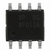
Z8F012ASB020SG Zilog, Z8F012ASB020SG Datasheet - Page 87

Z8F012ASB020SG
Manufacturer Part Number
Z8F012ASB020SG
Description
IC ENCORE XP MCU FLASH 1K 8SOIC
Manufacturer
Zilog
Series
Encore!® XP®r
Datasheet
1.Z8F011ASB020EG.pdf
(282 pages)
Specifications of Z8F012ASB020SG
Core Processor
Z8
Core Size
8-Bit
Speed
20MHz
Connectivity
IrDA, UART/USART
Peripherals
Brown-out Detect/Reset, LED, LVD, POR, PWM, Temp Sensor, WDT
Number Of I /o
6
Program Memory Size
1KB (1K x 8)
Program Memory Type
FLASH
Eeprom Size
16 x 8
Ram Size
256 x 8
Voltage - Supply (vcc/vdd)
2.7 V ~ 3.6 V
Data Converters
A/D 4x10b
Oscillator Type
Internal
Operating Temperature
0°C ~ 70°C
Package / Case
8-SOIC (3.9mm Width)
Processor Series
Z8F012Ax
Core
eZ8
Data Bus Width
8 bit
Data Ram Size
256 B
Interface Type
UART
Maximum Clock Frequency
20 MHz
Number Of Programmable I/os
6
Number Of Timers
2
Operating Supply Voltage
2.7 V to 3.6 V
Maximum Operating Temperature
+ 70 C
Mounting Style
SMD/SMT
Development Tools By Supplier
Z8F04A08100KITG, Z8F04A28100KITG, ZENETSC0100ZACG, ZENETSC0100ZACG, ZUSBOPTSC01ZACG, ZUSBSC00100ZAC, ZUSBSC00100ZACG
Minimum Operating Temperature
0 C
On-chip Adc
10 bit, 4 Channel
Lead Free Status / RoHS Status
Lead free / RoHS Compliant
Other names
269-4039
Z8F012ASB020SG
Z8F012ASB020SG
- Current page: 87 of 282
- Download datasheet (4Mb)
PS022825-0908
PWM DUAL OUTPUT Mode
In PWM DUAL OUTPUT mode, the timer outputs a Pulse-Width Modulated (PWM)
output signal pair (basic PWM signal and its complement) through two GPIO Port pins.
The timer input is the system clock. The timer first counts up to the 16-bit PWM match
value stored in the Timer PWM High and Low Byte registers. When the timer count value
matches the PWM value, the Timer Output toggles. The timer continues counting until it
reaches the Reload value stored in the Timer Reload High and Low Byte registers. Upon
reaching the Reload value, the timer generates an interrupt, the count value in the Timer
High and Low Byte registers is reset to
If the TPOL bit in the Timer Control register is set to 1, the Timer Output signal begins as
a High (1) and transitions to a Low (0) when the timer value matches the PWM value. The
Timer Output signal returns to a High (1) after the timer reaches the Reload value and is
reset to
If the TPOL bit in the Timer Control register is set to 0, the Timer Output signal begins as
a Low (0) and transitions to a High (1) when the timer value matches the PWM value. The
Timer Output signal returns to a Low (0) after the timer reaches the Reload value and is
reset to
The timer also generates a second PWM output signal Timer Output Complement. The
Timer Output Complement is the complement of the Timer Output PWM signal. A
programmable deadband delay can be configured to time delay (0 to 128 system clock
cycles) PWM output transitions on these two pins from a low to a high (inactive to active).
This ensures a time gap between the deassertion of one PWM output to the assertion of its
complement.
Follow the steps below for configuring a timer for PWM DUAL OUTPUT mode and initi-
ating the PWM operation:
1. Write to the Timer Control register to:
2. Write to the Timer High and Low Byte registers to set the starting count value
3. Write to the PWM High and Low Byte registers to set the PWM value.
4. Write to the PWM Control register to set the PWM dead band delay value. The
–
–
–
–
(typically
reset in PWM mode, counting always begins at the reset value of
deadband delay must be less than the duration of the positive phase of the PWM signal
(as defined by the PWM high and low byte registers). It must also be less than the
0001H
0001H
Disable the timer.
Configure the timer for PWM DUAL OUTPUT mode by writing the TMODE bits
in the TxCTL1 register and the TMODEHI bit in TxCTL0 register.
Set the prescale value.
Set the initial logic level (High or Low) and PWM High/Low transition for the
Timer Output alternate function.
0001H
.
.
). This only affects the first pass in PWM mode. After the first timer
0001H
and counting resumes.
Z8 Encore! XP
Product Specification
0001H
®
F082A Series
.
Timers
76
Related parts for Z8F012ASB020SG
Image
Part Number
Description
Manufacturer
Datasheet
Request
R

Part Number:
Description:
Communication Controllers, ZILOG INTELLIGENT PERIPHERAL CONTROLLER (ZIP)
Manufacturer:
Zilog, Inc.
Datasheet:

Part Number:
Description:
KIT DEV FOR Z8 ENCORE 16K TO 64K
Manufacturer:
Zilog
Datasheet:

Part Number:
Description:
KIT DEV Z8 ENCORE XP 28-PIN
Manufacturer:
Zilog
Datasheet:

Part Number:
Description:
DEV KIT FOR Z8 ENCORE 8K/4K
Manufacturer:
Zilog
Datasheet:

Part Number:
Description:
KIT DEV Z8 ENCORE XP 28-PIN
Manufacturer:
Zilog
Datasheet:

Part Number:
Description:
DEV KIT FOR Z8 ENCORE 4K TO 8K
Manufacturer:
Zilog
Datasheet:

Part Number:
Description:
CMOS Z8 microcontroller. ROM 16 Kbytes, RAM 256 bytes, speed 16 MHz, 32 lines I/O, 3.0V to 5.5V
Manufacturer:
Zilog, Inc.
Datasheet:

Part Number:
Description:
Low-cost microcontroller. 512 bytes ROM, 61 bytes RAM, 8 MHz
Manufacturer:
Zilog, Inc.
Datasheet:

Part Number:
Description:
Z8 4K OTP Microcontroller
Manufacturer:
Zilog, Inc.
Datasheet:

Part Number:
Description:
CMOS SUPER8 ROMLESS MCU
Manufacturer:
Zilog, Inc.
Datasheet:

Part Number:
Description:
SL1866 CMOSZ8 OTP Microcontroller
Manufacturer:
Zilog, Inc.
Datasheet:

Part Number:
Description:
SL1866 CMOSZ8 OTP Microcontroller
Manufacturer:
Zilog, Inc.
Datasheet:

Part Number:
Description:
OTP (KB) = 1, RAM = 125, Speed = 12, I/O = 14, 8-bit Timers = 2, Comm Interfaces Other Features = Por, LV Protect, Voltage = 4.5-5.5V
Manufacturer:
Zilog, Inc.
Datasheet:

Part Number:
Description:
Manufacturer:
Zilog, Inc.
Datasheet:


