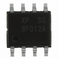
Z8F012ASB020SG Zilog, Z8F012ASB020SG Datasheet - Page 240

Z8F012ASB020SG
Manufacturer Part Number
Z8F012ASB020SG
Description
IC ENCORE XP MCU FLASH 1K 8SOIC
Manufacturer
Zilog
Series
Encore!® XP®r
Datasheet
1.Z8F011ASB020EG.pdf
(282 pages)
Specifications of Z8F012ASB020SG
Core Processor
Z8
Core Size
8-Bit
Speed
20MHz
Connectivity
IrDA, UART/USART
Peripherals
Brown-out Detect/Reset, LED, LVD, POR, PWM, Temp Sensor, WDT
Number Of I /o
6
Program Memory Size
1KB (1K x 8)
Program Memory Type
FLASH
Eeprom Size
16 x 8
Ram Size
256 x 8
Voltage - Supply (vcc/vdd)
2.7 V ~ 3.6 V
Data Converters
A/D 4x10b
Oscillator Type
Internal
Operating Temperature
0°C ~ 70°C
Package / Case
8-SOIC (3.9mm Width)
Processor Series
Z8F012Ax
Core
eZ8
Data Bus Width
8 bit
Data Ram Size
256 B
Interface Type
UART
Maximum Clock Frequency
20 MHz
Number Of Programmable I/os
6
Number Of Timers
2
Operating Supply Voltage
2.7 V to 3.6 V
Maximum Operating Temperature
+ 70 C
Mounting Style
SMD/SMT
Development Tools By Supplier
Z8F04A08100KITG, Z8F04A28100KITG, ZENETSC0100ZACG, ZENETSC0100ZACG, ZUSBOPTSC01ZACG, ZUSBSC00100ZAC, ZUSBSC00100ZACG
Minimum Operating Temperature
0 C
On-chip Adc
10 bit, 4 Channel
Lead Free Status / RoHS Status
Lead free / RoHS Compliant
Other names
269-4039
Z8F012ASB020SG
Z8F012ASB020SG
- Current page: 240 of 282
- Download datasheet (4Mb)
Table 131. Power-On Reset and Voltage Brownout Electrical Characteristics and Timing
Symbol
V
V
T
T
T
T
T
T
T
T
1
only and are not tested in production.
On-Chip Peripheral AC and DC Electrical Characteristics
PS022825-0908
Data in the typical column is from characterization at 3.3 V and 30 °C. These values are provided for design guidance
ANA
POR
POR
SMR
SMR
VBO
RAMP
SMP
POR
VBO
Parameter
Power-On Reset
Voltage Threshold
Voltage Brownout Reset
Voltage Threshold
V
Starting V
ensure valid Power-On
Reset.
Power-On Reset Analog
Delay
Power-On Reset Digital
Delay
Power-On Reset Digital
Delay
Stop Mode Recovery
with crystal oscillator
disabled
Stop Mode Recovery
with crystal oscillator
enabled
Voltage Brownout Pulse
Rejection Period
Time for V
transition from V
V
Reset
Stop Mode Recovery pin
pulse rejection period
POR
POR
to V
to ensure valid
DD
VBO
DD
voltage to
to
hysteresis
SS
to
Minimum Typical
2.20
2.15
0.10
–
–
–
T
A
= -40 °C to +105 °C
2.45
2.40
V
70
16
16
10
20
50
1
1
–
SS
1
Maximum
2.70
2.65
100
75
–
–
–
Units Conditions
Z8 Encore! XP
mV
ms
ms
ms
µs
µs
µs
µs
ns
V
V
V
V
V
V
Reset delay follows T
66 Internal Precision
Oscillator cycles + IPO
startup time (T
5000 Internal Precision
Oscillator cycles
66 Internal Precision
Oscillator cycles
5000 Internal Precision
Oscillator cycles
Period of time in which V
< V
a Reset.
For any SMR pin or for the
Reset pin when it is
asserted in STOP mode.
DD
DD
DD
Product Specification
VBO
= V
= V
> V
Electrical Characteristics
without generating
POR
VBO
POR
®
F082A Series
; T
IPOST
POR
Digital
)
ANA
DD
229
Related parts for Z8F012ASB020SG
Image
Part Number
Description
Manufacturer
Datasheet
Request
R

Part Number:
Description:
Communication Controllers, ZILOG INTELLIGENT PERIPHERAL CONTROLLER (ZIP)
Manufacturer:
Zilog, Inc.
Datasheet:

Part Number:
Description:
KIT DEV FOR Z8 ENCORE 16K TO 64K
Manufacturer:
Zilog
Datasheet:

Part Number:
Description:
KIT DEV Z8 ENCORE XP 28-PIN
Manufacturer:
Zilog
Datasheet:

Part Number:
Description:
DEV KIT FOR Z8 ENCORE 8K/4K
Manufacturer:
Zilog
Datasheet:

Part Number:
Description:
KIT DEV Z8 ENCORE XP 28-PIN
Manufacturer:
Zilog
Datasheet:

Part Number:
Description:
DEV KIT FOR Z8 ENCORE 4K TO 8K
Manufacturer:
Zilog
Datasheet:

Part Number:
Description:
CMOS Z8 microcontroller. ROM 16 Kbytes, RAM 256 bytes, speed 16 MHz, 32 lines I/O, 3.0V to 5.5V
Manufacturer:
Zilog, Inc.
Datasheet:

Part Number:
Description:
Low-cost microcontroller. 512 bytes ROM, 61 bytes RAM, 8 MHz
Manufacturer:
Zilog, Inc.
Datasheet:

Part Number:
Description:
Z8 4K OTP Microcontroller
Manufacturer:
Zilog, Inc.
Datasheet:

Part Number:
Description:
CMOS SUPER8 ROMLESS MCU
Manufacturer:
Zilog, Inc.
Datasheet:

Part Number:
Description:
SL1866 CMOSZ8 OTP Microcontroller
Manufacturer:
Zilog, Inc.
Datasheet:

Part Number:
Description:
SL1866 CMOSZ8 OTP Microcontroller
Manufacturer:
Zilog, Inc.
Datasheet:

Part Number:
Description:
OTP (KB) = 1, RAM = 125, Speed = 12, I/O = 14, 8-bit Timers = 2, Comm Interfaces Other Features = Por, LV Protect, Voltage = 4.5-5.5V
Manufacturer:
Zilog, Inc.
Datasheet:

Part Number:
Description:
Manufacturer:
Zilog, Inc.
Datasheet:


