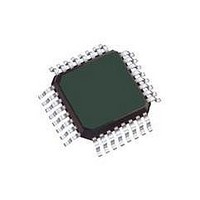
MCHC908GR8AMFAE Freescale Semiconductor, MCHC908GR8AMFAE Datasheet - Page 234

MCHC908GR8AMFAE
Manufacturer Part Number
MCHC908GR8AMFAE
Description
IC MCU 8K FLASH 8MHZ 32-LQFP
Manufacturer
Freescale Semiconductor
Series
HC08r
Datasheet
1.MCHC908GR8ACFAE.pdf
(260 pages)
Specifications of MCHC908GR8AMFAE
Core Processor
HC08
Core Size
8-Bit
Speed
8MHz
Connectivity
SCI, SPI
Peripherals
LVD, POR, PWM
Number Of I /o
21
Program Memory Size
7.5KB (7.5K x 8)
Program Memory Type
FLASH
Ram Size
384 x 8
Voltage - Supply (vcc/vdd)
2.7 V ~ 5.5 V
Data Converters
A/D 6x8b
Oscillator Type
Internal
Operating Temperature
-40°C ~ 125°C
Package / Case
32-LQFP
Processor Series
HC08G
Core
HC08
Data Bus Width
8 bit
Data Ram Size
384 B
Interface Type
SCI, SPI
Maximum Clock Frequency
8.2 MHz
Number Of Programmable I/os
21
Number Of Timers
3
Maximum Operating Temperature
+ 125 C
Mounting Style
SMD/SMT
Development Tools By Supplier
FSICEBASE, DEMO908GZ60E, M68CBL05CE, M68EML08GPGTE
Minimum Operating Temperature
- 40 C
On-chip Adc
8 bit, 6 Channel
Lead Free Status / RoHS Status
Lead free / RoHS Compliant
Eeprom Size
-
Lead Free Status / Rohs Status
Details
Available stocks
Company
Part Number
Manufacturer
Quantity
Price
Company:
Part Number:
MCHC908GR8AMFAE
Manufacturer:
Freescale Semiconductor
Quantity:
10 000
Company:
Part Number:
MCHC908GR8AMFAER
Manufacturer:
Freescale Semiconductor
Quantity:
10 000
- Current page: 234 of 260
- Download datasheet (4Mb)
Electrical Specifications
19.6 3.0 V DC Electrical Characteristics
234
POR reset voltage
POR rise time ramp rate
Output high voltage
Output low voltage
Input high voltage
Input low voltage
1. V
2. Typical values reflect average measurements at midpoint of voltage range, 25 °C only.
3. Run (operating) I
4. Wait I
5. Stop I
6. Stop I
7. Pullups and pulldowns are disabled. Port B leakage is specified in
8. Maximum is highest voltage that POR is possible.
9. If minimum V
(I
(I
(I
Maximum combined I
Maximum combined I
Maximum total I
(I
(I
(I
Maximum combined I
Maximum combined I
All ports, IRQs, RESET
OSC1
All ports, IRQs, RESET
OSC1
Maximum total I
loads. Less than 100 pF on all outputs. C
affects run I
than 100 pF on all outputs. C
I
No dc loads. Less than 100 pF on all outputs. All inputs configured as inputs.
V
Load
Load
Load
port PTD0–PTD3
port A, port B
Load
Load
Load
port PTD0–PTD3
port A, port B
DD
DD
DD
. Measured with PLL and LVI enabled.
= 5.0 Vdc
is reached.
DD
DD
DD
= –0.6 mA) all I/O pins
= –4.0 mA) all I/O pins
= –4.0 mA) pins PTC0–PTC1 only
= 0.5 mA) all I/O pins
= 6.0 mA) all I/O pins
= 10.0 mA) pins PTC0–PTC1 only
measured using external square wave clock source (f
is measured with OSC1 = V
with TBM enabled is measured using an external crystal clock source (f
DD
DD
. Measured with all modules enabled.
±
OH
(8)
OL
is not reached before the internal POR reset is released, RST must be driven low externally until minimum
DD
10%, V
Characteristic
Characteristic
for all port pins
for all port pins
measured using external square wave clock source (f
OH
OH
OL
OL
(9)
for port C, port E,
for port PTD4–PTD6,
for port C, port E,
for port PTD4–PTD6,
SS
= 0 Vdc, T
MC68HC908GR8A • MC68HC908GR4A Data Sheet, Rev. 5
L
= 20 pF on OSC2. All ports configured as inputs. OSC2 capacitance linearly affects wait
(1)
(1)
SS
A
.
= T
L
= 20 pF on OSC2. All ports configured as inputs. OSC2 capacitance linearly
L
to T
H
, unless otherwise noted
V
Symbol
Symbol
PORRST
R
osc
I
I
I
V
V
V
I
I
V
V
V
I
OH1
OH2
OHT
V
OL1
OL2
V
OLT
POR
OH
OH
OH
OL
OL
OL
IH
IL
= 32.8 MHz). All inputs 0.2 V from rail. No dc loads. Less
19.12 ADC
osc
V
V
V
0.7 x V
0.8 x V
DD
DD
DD
0.035
= 32.8 MHz). All inputs 0.2 V from rail. No dc
V
Min
Min
—
—
—
—
—
—
—
—
—
0
SS
Characteristics.
– 0.3
– 1.0
– 0.5
OSC
DD
DD
= 8 MHz). All inputs 0.2 V from rail.
Typ
Typ
700
—
—
—
—
—
—
—
—
—
—
—
—
—
—
—
(2)
(2)
Freescale Semiconductor
Continued on next page
0.3 x V
0.2 x V
Max
Max
V
800
0.3
1.0
0.8
30
30
60
30
30
60
—
—
—
—
DD
DD
DD
V/ms
Unit
Unit
mV
mA
mA
mA
mA
mA
mA
V
V
V
V
V
V
V
V
Related parts for MCHC908GR8AMFAE
Image
Part Number
Description
Manufacturer
Datasheet
Request
R
Part Number:
Description:
Manufacturer:
Freescale Semiconductor, Inc
Datasheet:
Part Number:
Description:
Manufacturer:
Freescale Semiconductor, Inc
Datasheet:
Part Number:
Description:
Manufacturer:
Freescale Semiconductor, Inc
Datasheet:
Part Number:
Description:
Manufacturer:
Freescale Semiconductor, Inc
Datasheet:
Part Number:
Description:
Manufacturer:
Freescale Semiconductor, Inc
Datasheet:
Part Number:
Description:
Manufacturer:
Freescale Semiconductor, Inc
Datasheet:
Part Number:
Description:
Manufacturer:
Freescale Semiconductor, Inc
Datasheet:
Part Number:
Description:
Manufacturer:
Freescale Semiconductor, Inc
Datasheet:
Part Number:
Description:
Manufacturer:
Freescale Semiconductor, Inc
Datasheet:
Part Number:
Description:
Manufacturer:
Freescale Semiconductor, Inc
Datasheet:
Part Number:
Description:
Manufacturer:
Freescale Semiconductor, Inc
Datasheet:
Part Number:
Description:
Manufacturer:
Freescale Semiconductor, Inc
Datasheet:
Part Number:
Description:
Manufacturer:
Freescale Semiconductor, Inc
Datasheet:
Part Number:
Description:
Manufacturer:
Freescale Semiconductor, Inc
Datasheet:
Part Number:
Description:
Manufacturer:
Freescale Semiconductor, Inc
Datasheet:


