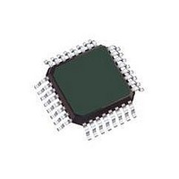
MCHC908GR8AMFAE Freescale Semiconductor, MCHC908GR8AMFAE Datasheet - Page 55

MCHC908GR8AMFAE
Manufacturer Part Number
MCHC908GR8AMFAE
Description
IC MCU 8K FLASH 8MHZ 32-LQFP
Manufacturer
Freescale Semiconductor
Series
HC08r
Datasheet
1.MCHC908GR8ACFAE.pdf
(260 pages)
Specifications of MCHC908GR8AMFAE
Core Processor
HC08
Core Size
8-Bit
Speed
8MHz
Connectivity
SCI, SPI
Peripherals
LVD, POR, PWM
Number Of I /o
21
Program Memory Size
7.5KB (7.5K x 8)
Program Memory Type
FLASH
Ram Size
384 x 8
Voltage - Supply (vcc/vdd)
2.7 V ~ 5.5 V
Data Converters
A/D 6x8b
Oscillator Type
Internal
Operating Temperature
-40°C ~ 125°C
Package / Case
32-LQFP
Processor Series
HC08G
Core
HC08
Data Bus Width
8 bit
Data Ram Size
384 B
Interface Type
SCI, SPI
Maximum Clock Frequency
8.2 MHz
Number Of Programmable I/os
21
Number Of Timers
3
Maximum Operating Temperature
+ 125 C
Mounting Style
SMD/SMT
Development Tools By Supplier
FSICEBASE, DEMO908GZ60E, M68CBL05CE, M68EML08GPGTE
Minimum Operating Temperature
- 40 C
On-chip Adc
8 bit, 6 Channel
Lead Free Status / RoHS Status
Lead free / RoHS Compliant
Eeprom Size
-
Lead Free Status / Rohs Status
Details
Available stocks
Company
Part Number
Manufacturer
Quantity
Price
Company:
Part Number:
MCHC908GR8AMFAE
Manufacturer:
Freescale Semiconductor
Quantity:
10 000
Company:
Part Number:
MCHC908GR8AMFAER
Manufacturer:
Freescale Semiconductor
Quantity:
10 000
- Current page: 55 of 260
- Download datasheet (4Mb)
Chapter 4
Clock Generator Module (CGM)
4.1 Introduction
This section describes the clock generator module. The CGM generates the crystal clock signal,
CGMXCLK, which operates at the frequency of the crystal. The CGM also generates the base clock
signal, CGMOUT, which is based on either the crystal clock divided by two or the phase-locked loop (PLL)
clock, CGMVCLK, divided by two. In user mode, CGMOUT is the clock from which the SIM derives the
system clocks, including the bus clock, which is at a frequency of CGMOUT/2. The PLL is a fully functional
frequency generator designed for use with crystals or ceramic resonators. The PLL can generate an
8-MHz bus frequency using a 1–8 MHz crystal or external clock source.
4.2 Features
Features of the CGM include:
4.3 Functional Description
The CGM consists of three major submodules:
Figure 4-1
Freescale Semiconductor
•
•
•
•
•
•
•
•
•
•
Phase-locked loop with output frequency in integer multiples of an integer dividend of the crystal
reference
High-frequency crystal operation with low-power operation and high-output frequency resolution
Programmable hardware voltage-controlled oscillator (VCO) for low-jitter operation
Automatic bandwidth control mode for low-jitter operation
Automatic frequency lock detector
CPU interrupt on entry or exit from locked condition
Configuration register bit to allow oscillator operation during stop mode
Crystal oscillator circuit — The crystal oscillator circuit generates the constant crystal frequency
clock, CGMXCLK.
Phase-locked loop (PLL) — The PLL generates the programmable VCO frequency clock,
CGMVCLK.
Base clock selector circuit — This software-controlled circuit selects either CGMXCLK divided by
two or the VCO clock, CGMVCLK, divided by two as the base clock, CGMOUT. The SIM derives
the system clocks from either CGMOUT or CGMXCLK.
shows the structure of the CGM.
MC68HC908GR8A • MC68HC908GR4A Data Sheet, Rev. 5
55
Related parts for MCHC908GR8AMFAE
Image
Part Number
Description
Manufacturer
Datasheet
Request
R
Part Number:
Description:
Manufacturer:
Freescale Semiconductor, Inc
Datasheet:
Part Number:
Description:
Manufacturer:
Freescale Semiconductor, Inc
Datasheet:
Part Number:
Description:
Manufacturer:
Freescale Semiconductor, Inc
Datasheet:
Part Number:
Description:
Manufacturer:
Freescale Semiconductor, Inc
Datasheet:
Part Number:
Description:
Manufacturer:
Freescale Semiconductor, Inc
Datasheet:
Part Number:
Description:
Manufacturer:
Freescale Semiconductor, Inc
Datasheet:
Part Number:
Description:
Manufacturer:
Freescale Semiconductor, Inc
Datasheet:
Part Number:
Description:
Manufacturer:
Freescale Semiconductor, Inc
Datasheet:
Part Number:
Description:
Manufacturer:
Freescale Semiconductor, Inc
Datasheet:
Part Number:
Description:
Manufacturer:
Freescale Semiconductor, Inc
Datasheet:
Part Number:
Description:
Manufacturer:
Freescale Semiconductor, Inc
Datasheet:
Part Number:
Description:
Manufacturer:
Freescale Semiconductor, Inc
Datasheet:
Part Number:
Description:
Manufacturer:
Freescale Semiconductor, Inc
Datasheet:
Part Number:
Description:
Manufacturer:
Freescale Semiconductor, Inc
Datasheet:
Part Number:
Description:
Manufacturer:
Freescale Semiconductor, Inc
Datasheet:


