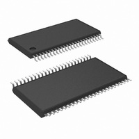
COP8CCR9IMT8/NOPB National Semiconductor, COP8CCR9IMT8/NOPB Datasheet - Page 17

COP8CCR9IMT8/NOPB
Manufacturer Part Number
COP8CCR9IMT8/NOPB
Description
IC MCU EEPROM 8BIT 32K 48-TSSOP
Manufacturer
National Semiconductor
Series
COP8™ 8Cr
Datasheet
1.COP8CDR9HVA8NOPB.pdf
(84 pages)
Specifications of COP8CCR9IMT8/NOPB
Core Processor
COP8
Core Size
8-Bit
Speed
20MHz
Connectivity
Microwire/Plus (SPI), UART/USART
Peripherals
Brown-out Detect/Reset, POR, PWM, WDT
Number Of I /o
39
Program Memory Size
32KB (32K x 8)
Program Memory Type
FLASH
Ram Size
1K x 8
Voltage - Supply (vcc/vdd)
2.7 V ~ 5.5 V
Data Converters
A/D 16x10b
Oscillator Type
Internal
Operating Temperature
-40°C ~ 85°C
Package / Case
48-TSSOP
Data Bus Width
8 bit
Maximum Clock Frequency
20 MHz
Data Ram Size
1 KB
On-chip Adc
10 bit, 16 channel
Number Of Programmable I/os
59
Number Of Timers
3
Height
0.9 mm
Interface Type
SPI, USART
Length
12.5 mm
Maximum Operating Temperature
+ 85 C
Minimum Operating Temperature
- 40 C
Supply Voltage (max)
5.5 V
Supply Voltage (min)
2.7 V
Width
6.1 mm
Lead Free Status / RoHS Status
Lead free / RoHS Compliant
Eeprom Size
-
Lead Free Status / Rohs Status
Details
Other names
*COP8CCR9IMT8
*COP8CCR9IMT8/NOPB
COP8CCR9IMT8
*COP8CCR9IMT8/NOPB
COP8CCR9IMT8
8.0 Electrical Characteristics
AC Electrical Characteristics (−40˚C ≤ T
Resolution
DNL
INL
Offset Error
Gain Error
Input Voltage Range
Analog Input Leakage Current
Analog Input Resistance (Note 9)
Analog Input Capacitance
Conversion Clock Period
Conversion Time (including S/H Time)
Operating Current on AV
Note 11: Supply and IDLE currents are measured with CKI driven with a square wave Oscillator, CKO driven 180˚ out of phase with CKI, inputs connected to V
and outputs driven low but not connected to a load.
Note 12: The HALT mode will stop CKI from oscillating. Measurement of I
G0, and G2–G5 programmed as low outputs and not driving a load; all D outputs programmed low and not driving a load; all inputs tied to V
clock monitor and BOR disabled. Parameter refers to HALT mode entered via setting bit 7 of the G Port data register.
Note 13: Pins G6 and RESET are designed with a high voltage input network. These pins allow input voltages
when biased at voltages
must be limited to
Note 14: If timer is in high speed mode, the minimum time is 1 MCLK. If timer is not in high speed mode, the minimum time is 1 t
Note 15: Absolute Maximum Ratings should not be exceeded.
Note 16: V
A/D Converter Electrical Characteristics (−40˚C ≤ T
(Single-ended mode only)
Note 17: Resistance between the device input and the internal sample and hold capacitance.
Datasheet min/max specification limits are guaranteed by design, test, or statistical analysis.
cc
must be valid and stable before G6 is raised to a high voltage.
<
Parameter
(V
CC
>
+ 7V. WARNING: Voltages in excess of 14V will cause damage to the pins. This warning excludes ESD transients.
V
CC
CC
(the pins do not have source current when biased at a voltage below V
FIGURE 1. MICROWIRE/PLUS Timing
V
V
V
V
4.5V ≤ V
4.5V ≤ V
AV
CC
CC
CC
CC
CC
(Continued)
= 5V
= 5V
= 5V
= 5V
Conditions
= 5.5V
CC
CC
<
<
DD
5.5V
5.5V
HALT is done with device neither sourcing nor sinking current; with L. A. B, C, E, F,
17
A
≤ +125˚C)
Min
0.8
0
CC
). These two pins will not latch up. The voltage at the pins
Typ
0.2
A
15
(Continued)
>
≤ +125˚C)
V
CC
and the pins will have sink current to V
10137405
+0.5, −2.5
+2.5, −1
Max
V
0.5
0.6
±
±
10
6k
30
CC
7
C
1
3
.
CC
; A/D converter and
Conversion
www.national.com
Cycles
Units
Clock
LSB
LSB
LSB
LSB
Bits
A/D
mA
µA
pF
µs
V
Ω
CC
CC


