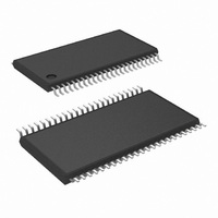
COP8CCR9IMT8/NOPB National Semiconductor, COP8CCR9IMT8/NOPB Datasheet - Page 20

COP8CCR9IMT8/NOPB
Manufacturer Part Number
COP8CCR9IMT8/NOPB
Description
IC MCU EEPROM 8BIT 32K 48-TSSOP
Manufacturer
National Semiconductor
Series
COP8™ 8Cr
Datasheet
1.COP8CDR9HVA8NOPB.pdf
(84 pages)
Specifications of COP8CCR9IMT8/NOPB
Core Processor
COP8
Core Size
8-Bit
Speed
20MHz
Connectivity
Microwire/Plus (SPI), UART/USART
Peripherals
Brown-out Detect/Reset, POR, PWM, WDT
Number Of I /o
39
Program Memory Size
32KB (32K x 8)
Program Memory Type
FLASH
Ram Size
1K x 8
Voltage - Supply (vcc/vdd)
2.7 V ~ 5.5 V
Data Converters
A/D 16x10b
Oscillator Type
Internal
Operating Temperature
-40°C ~ 85°C
Package / Case
48-TSSOP
Data Bus Width
8 bit
Maximum Clock Frequency
20 MHz
Data Ram Size
1 KB
On-chip Adc
10 bit, 16 channel
Number Of Programmable I/os
59
Number Of Timers
3
Height
0.9 mm
Interface Type
SPI, USART
Length
12.5 mm
Maximum Operating Temperature
+ 85 C
Minimum Operating Temperature
- 40 C
Supply Voltage (max)
5.5 V
Supply Voltage (min)
2.7 V
Width
6.1 mm
Lead Free Status / RoHS Status
Lead free / RoHS Compliant
Eeprom Size
-
Lead Free Status / Rohs Status
Details
Other names
*COP8CCR9IMT8
*COP8CCR9IMT8/NOPB
COP8CCR9IMT8
*COP8CCR9IMT8/NOPB
COP8CCR9IMT8
www.national.com
9.0 Pin Descriptions
9.1 EMULATION CONNECTION
Connection to the emulation system is made via a 2 x 7
connector which interrupts the continuity of the RESET, G0,
G1, G2 and G3 signals between the COP8 device and the
rest of the target system (as shown in Figure 6). This con-
nector can be designed into the production pc board and can
be replaced by jumpers or signal traces when emulation is
no longer necessary. The emulator will replicate all functions
of G0 - G3 and RESET. For proper operation, no connection
should be made on the device side of the emulator connec-
tor.
10.0 Functional Description
The architecture of the device is a modified Harvard archi-
tecture. With the Harvard architecture, the program memory
(Flash) is separate from the data store memory (RAM). Both
Program Memory and Data Memory have their own separate
FIGURE 5. I/O Port Configurations — Input Mode
FIGURE 6. Emulation Connection
(Continued)
10137409
10137408
20
addressing space with separate address buses. The archi-
tecture, though based on the Harvard architecture, permits
transfer of data from Flash Memory to RAM.
10.1 CPU REGISTERS
The CPU can do an 8-bit addition, subtraction, logical or shift
operation in one instruction (t
There are six CPU registers:
A is the 8-bit Accumulator Register
PC is the 15-bit Program Counter Register
B is an 8-bit RAM address pointer, which can be optionally
post auto incremented or decremented.
X is an 8-bit alternate RAM address pointer, which can be
optionally post auto incremented or decremented.
S is the 8-bit Data Segment Address Register used to extend
the lower half of the address range (00 to 7F) into 256 data
segments of 128 bytes each.
SP is the 8-bit stack pointer, which points to the subroutine/
interrupt stack (in RAM). With reset the SP is initialized to
RAM address 06F Hex. The SP is decremented as items are
pushed onto the stack. SP points to the next available loca-
tion on the stack.
All the CPU registers are memory mapped with the excep-
tion of the Accumulator (A) and the Program Counter (PC).
10.2 PROGRAM MEMORY
The program memory consists of 32,768 bytes of Flash
Memory. These bytes may hold program instructions or con-
stant data (data tables for the LAID instruction, jump vectors
for the JID instruction, and interrupt vectors for the VIS
instruction). The program memory is addressed by the 15-bit
program counter (PC). All interrupts in the device vector to
program memory location 00FF Hex. The program memory
reads 00 Hex in the erased state. Program execution starts
at location 0 after RESET.
If a Return instruction is executed when the SP contains 6F
(hex), instruction execution will continue from Program
Memory location 7FFF (hex). If location 7FFF is accessed by
an instruction fetch, the Flash Memory will return a value of
00. This is the opcode for the INTR instruction and will cause
a Software Trap.
For the purpose of erasing and rewriting the Flash Memory,
it is organized in pages of 128 bytes.
10.3 DATA MEMORY
The data memory address space includes the on-chip RAM
and data registers, the I/O registers (Configuration, Data and
Pin), the control registers, the MICROWIRE/PLUS SIO shift
register, and the various registers, and counters associated
with the timers and the USART (with the exception of the
IDLE timer). Data memory is addressed directly by the in-
struction or indirectly by the B, X and SP pointers.
The data memory consists of 1024 bytes of RAM. Sixteen
bytes of RAM are mapped as “registers” at addresses 0F0 to
0FF Hex. These registers can be loaded immediately, and
also decremented and tested with the DRSZ (decrement
register and skip if zero) instruction. The memory pointer
registers X, SP, B and S are memory mapped into this space
at address locations 0FC to 0FF Hex respectively, with the
other registers being available for general usage.
PU is the upper 7 bits of the program counter (PC)
PL is the lower 8 bits of the program counter (PC)
C
) cycle time.


