COP8CCR9IMT8/NOPB National Semiconductor, COP8CCR9IMT8/NOPB Datasheet - Page 43
COP8CCR9IMT8/NOPB
Manufacturer Part Number
COP8CCR9IMT8/NOPB
Description
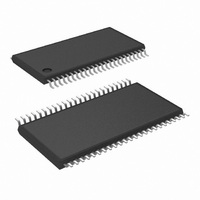
IC MCU EEPROM 8BIT 32K 48-TSSOP
Manufacturer
National Semiconductor
Series
COP8™ 8Cr
Datasheet
1.COP8CDR9HVA8NOPB.pdf
(84 pages)
Specifications of COP8CCR9IMT8/NOPB
Core Processor
COP8
Core Size
8-Bit
Speed
20MHz
Connectivity
Microwire/Plus (SPI), UART/USART
Peripherals
Brown-out Detect/Reset, POR, PWM, WDT
Number Of I /o
39
Program Memory Size
32KB (32K x 8)
Program Memory Type
FLASH
Ram Size
1K x 8
Voltage - Supply (vcc/vdd)
2.7 V ~ 5.5 V
Data Converters
A/D 16x10b
Oscillator Type
Internal
Operating Temperature
-40°C ~ 85°C
Package / Case
48-TSSOP
Data Bus Width
8 bit
Maximum Clock Frequency
20 MHz
Data Ram Size
1 KB
On-chip Adc
10 bit, 16 channel
Number Of Programmable I/os
59
Number Of Timers
3
Height
0.9 mm
Interface Type
SPI, USART
Length
12.5 mm
Maximum Operating Temperature
+ 85 C
Minimum Operating Temperature
- 40 C
Supply Voltage (max)
5.5 V
Supply Voltage (min)
2.7 V
Width
6.1 mm
Lead Free Status / RoHS Status
Lead free / RoHS Compliant
Eeprom Size
-
Lead Free Status / Rohs Status
Details
Other names
*COP8CCR9IMT8
*COP8CCR9IMT8/NOPB
COP8CCR9IMT8
*COP8CCR9IMT8/NOPB
COP8CCR9IMT8


13.0 Power Saving Features
The IDLE mode uses the on-chip IDLE Timer (Timer T0) to
keep track of elapsed time in the IDLE state. The IDLE Timer
runs continuously at the low speed clock rate, whether or not
the device is in the IDLE mode. Each time the bit of the timer
associated with the selected window toggles, the T0PND bit
is set, an interrupt is generated (if enabled), and the device
exits the IDLE mode if in that mode. If the IDLE Timer
interrupt is enabled, the interrupt is serviced before execu-
tion of the main program resumes. (However, the instruction
which was started as the part entered the IDLE mode is
completed before the interrupt is serviced. This instruction
should be a NOP which should follow the enter IDLE instruc-
tion.) The user must reset the IDLE Timer pending flag
(T0PND) before entering the IDLE mode.
As with the HALT mode, this device can also be returned to
normal operation with a Multi-Input Wake-up input.
The IDLE Timer cannot be started or stopped under software
control, and it is not memory mapped, so it cannot be read or
written by the software. Its state upon Reset is unknown.
Therefore, if the device is put into the IDLE mode at an
arbitrary time, it will stay in the IDLE mode for somewhere
between 30 µs and the selected time period.
In order to precisely time the duration of the IDLE state, entry
into the IDLE mode must be ”synchronized to the state of the
IDLE Timer. The best way to do this is to use the IDLE Timer
interrupt, which occurs on every underflow of the bit of the
IDLE Timer which is associated with the selected window.
Another method is to poll the state of the IDLE Timer pending
bit T0PND, which is set on the same occurrence. The Idle
Timer interrupt is enabled by setting bit T0EN in the ICNTRL
register.
Any time the IDLE Timer window length is changed there is
the possibility of generating a spurious IDLE Timer interrupt
by setting the T0PND bit. The user is advised to disable
IDLE Timer interrupts prior to changing the value of the
ITSEL bits of the ITMR Register and then clear the T0PND
bit before attempting to synchronize operation to the IDLE
Timer.
Note: As with the HALT mode, it is necessary to program two
NOP’s to allow clock resynchronization upon return from the
IDLE mode. The NOP’s are placed either at the beginning of
the IDLE Timer interrupt routine or immediately following the
“enter IDLE mode” instruction.
For more information on the IDLE Timer and its associated
interrupt, see the description in the Timers section.
13.5 LOW SPEED MODE OPERATION
This mode of operation allows for low speed operation of the
core clock and low speed operation of the Idle Timer. Be-
cause the low speed oscillator draws very little operating
current, and also to expedite restarting from HALT mode, the
low speed oscillator is left on at all times in this mode,
including HALT mode. This is the lowest power mode of
operation on the device. This mode can only be entered from
the Dual Clock mode.
To enter the Low Speed mode, the following sequence must
be followed using two separate instructions:
1. Software sets the CCKSEL bit to 1.
2. Software clears the HSON bit to 0.
Since the low speed oscillator is already running, there is no
clock startup delay.
(Continued)
43
13.5.1 Low Speed HALT Mode
The fully static architecture of this device allows the state of
the microcontroller to be frozen. Because the low speed
oscillator draws very minimal operating current, it will be left
running in the low speed halt mode. However, the Idle Timer
will not be running. This also allows for a faster exit from
HALT. The processor can be forced to exit the HALT mode
and resume normal operation at any time.
During normal operation, the actual power consumption de-
pends heavily on the clock speed and operating voltage
used in an application and is shown in the Electrical Speci-
fications. In the HALT mode, the device only draws a small
leakage current, plus current for the BOR feature (if en-
abled), plus the 32 kHz oscillator current, plus any current
necessary for driving the outputs. Since total power con-
sumption is affected by the amount of current required to
drive the outputs, all I/Os should be configured to draw
minimal current prior to entering the HALT mode, if possible.
13.5.1.1 Entering The Low Speed Halt Mode
The device enters the HALT mode under software control
when the Port G data register bit 7 is set to 1. All processor
action stops in the middle of the next instruction cycle, and
power consumption is reduced to a very low level. In order to
expedite exit from HALT, the low speed oscillator is left
running when the device is Halted in the Low Speed mode.
However, the Idle Timer will not be clocked.
13.5.1.2 Exiting The Low Speed Halt Mode
When the HALT mode is entered by setting bit 7 of the Port
G data register, there is a choice of methods for exiting the
HALT mode: a chip Reset using the RESET pin or a Multi-
Input Wake-up. The Reset method and Multi-Input Wake-up
method can be used with any clock option, but the availabil-
ity of the G7 input is dependent on the clock option.
13.5.1.3 HALT Exit Using Reset
A device Reset, which is invoked by a low-level signal on the
RESET input pin, takes the device out of the Low Speed
mode and puts it into the High Speed mode.
13.5.1.4 HALT Exit Using Multi-Input Wake-up
The device can be brought out of the HALT mode by a
transition received on one of the available Wake-up pins.
The pins used and the types of transitions sensed on the
Multi-input pins are software programmable. For information
on programming and using the Multi-Input Wake-up feature,
refer to the Multi-Input Wake-up section.
As the low speed oscillator is left running, there is no start up
delay when exiting the low speed halt mode, regardless of
the state of the CLKDLY bit.
Note: To ensure accurate operation upon start-up of the
device using Multi-input Wake-up, the instruction in the ap-
plication program used for entering the HALT mode should
be followed by two consecutive NOP (no-operation) instruc-
tions.
13.5.1.5 Options
This device has two options associated with the HALT mode.
The first option enables the HALT mode feature, while the
second option disables HALT mode operation. Selecting the
disable HALT mode option will cause the microcontroller to
ignore any attempts to HALT the device under software
control. See the Option section for more details on this
option bit.
www.national.com
Related parts for COP8CCR9IMT8/NOPB
Image
Part Number
Description
Manufacturer
Datasheet
Request
R

Part Number:
Description:
National Semiconductor [8-Bit D/A Converter]
Manufacturer:
National Semiconductor
Datasheet:
Part Number:
Description:
National Semiconductor [Media Coprocessor]
Manufacturer:
National Semiconductor
Datasheet:
Part Number:
Description:
Digitally Controlled Tone and Volume Circuit with Stereo Audio Power Amplifier, Microphone Preamp Stage and National 3D Sound
Manufacturer:
National Semiconductor
Datasheet:
Part Number:
Description:
Digitally Controlled Tone and Volume Circuit with Stereo Audio Power Amplifier, Microphone Preamp Stage and National 3D Sound
Manufacturer:
National Semiconductor
Datasheet:
Part Number:
Description:
AC97 Rev 2 Codec with Sample Rate Conversion and National 3D Sound
Manufacturer:
National Semiconductor
Part Number:
Description:
Manufacturer:
National Semiconductor
Datasheet:
Part Number:
Description:
Manufacturer:
National Semiconductor
Datasheet:
Part Number:
Description:
General Purpose, Low Voltage, Low Power, Rail-to-Rail Output Operational Amplifiers
Manufacturer:
National Semiconductor
Datasheet:
Part Number:
Description:
8-bit 20 MSPS flash A/D converter.
Manufacturer:
National Semiconductor
Datasheet:
Part Number:
Description:
Low Noise Quad Operational Amplifier
Manufacturer:
National Semiconductor
Datasheet:
Part Number:
Description:
Quad Differential Line Receivers
Manufacturer:
National Semiconductor
Datasheet:
Part Number:
Description:
Quad High Speed Trapezoidal? Bus Transceiver
Manufacturer:
National Semiconductor
Datasheet:
Part Number:
Description:
Dual Line Receiver
Manufacturer:
National Semiconductor
Datasheet:
Part Number:
Description:
TTL to 10k ECL Level Translator with Latch
Manufacturer:
National Semiconductor
Datasheet: