COP8CCR9IMT8/NOPB National Semiconductor, COP8CCR9IMT8/NOPB Datasheet - Page 36
COP8CCR9IMT8/NOPB
Manufacturer Part Number
COP8CCR9IMT8/NOPB
Description
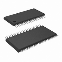
IC MCU EEPROM 8BIT 32K 48-TSSOP
Manufacturer
National Semiconductor
Series
COP8™ 8Cr
Datasheet
1.COP8CDR9HVA8NOPB.pdf
(84 pages)
Specifications of COP8CCR9IMT8/NOPB
Core Processor
COP8
Core Size
8-Bit
Speed
20MHz
Connectivity
Microwire/Plus (SPI), UART/USART
Peripherals
Brown-out Detect/Reset, POR, PWM, WDT
Number Of I /o
39
Program Memory Size
32KB (32K x 8)
Program Memory Type
FLASH
Ram Size
1K x 8
Voltage - Supply (vcc/vdd)
2.7 V ~ 5.5 V
Data Converters
A/D 16x10b
Oscillator Type
Internal
Operating Temperature
-40°C ~ 85°C
Package / Case
48-TSSOP
Data Bus Width
8 bit
Maximum Clock Frequency
20 MHz
Data Ram Size
1 KB
On-chip Adc
10 bit, 16 channel
Number Of Programmable I/os
59
Number Of Timers
3
Height
0.9 mm
Interface Type
SPI, USART
Length
12.5 mm
Maximum Operating Temperature
+ 85 C
Minimum Operating Temperature
- 40 C
Supply Voltage (max)
5.5 V
Supply Voltage (min)
2.7 V
Width
6.1 mm
Lead Free Status / RoHS Status
Lead free / RoHS Compliant
Eeprom Size
-
Lead Free Status / Rohs Status
Details
Other names
*COP8CCR9IMT8
*COP8CCR9IMT8/NOPB
COP8CCR9IMT8
*COP8CCR9IMT8/NOPB
COP8CCR9IMT8


www.national.com
12.0 Timers
12.1.1 ITMR Register
Bits 7–4: Described in 13.0 Power Saving Features.
Note: Documentation for previous COP8 devices, which in-
cluded the Programmable Idle Timer, recommended the user
write zero to the high order bits of the ITMR Register. If
existing programs are updated to use this device, writing
zero to these bits will cause the device to reset (see 13.0
Power Saving Features).
RSVD: This bit is reserved and must be set to 0.
ITSEL2:0: Selects the Idle Timer period as described in
Table 14, Idle Timer Window Length.
Any time the IDLE Timer period is changed there is the
possibility of generating a spurious IDLE Timer interrupt by
setting the T0PND bit. The user is advised to disable IDLE
Timer interrupts prior to changing the value of the ITSEL bits
of the ITMR Register and then clear the T0PND bit before
attempting to synchronize operation to the IDLE Timer.
12.2 TIMER T1, TIMER T2, AND TIMER T3
The device has a set of three powerful timer/counter blocks,
T1, T2, and T3. Since T1, T2 and T3 are identical, except for
the high speed operation of T2 and T3, all comments are
equally applicable to any of the three timer blocks which will
be referred to as Tx. Differences between the timers will be
specifically noted.
Each timer block consists of a 16-bit timer, Tx, and two
supporting 16-bit autoreload/capture registers, RxA and
RxB. Each timer block has two pins associated with it, TxA
and TxB. The pin TxA supports I/O required by the timer
block, while the pin TxB is an input to the timer block. The
timer block has three operating modes: Processor Indepen-
dent PWM mode, External Event Counter mode, and Input
Capture mode.
The control bits TxC3, TxC2, and TxC1 allow selection of the
different modes of operation.
12.2.1 Timer Operating Speeds
Each of the Tx timers, except T1, have the ability to operate
at either the instruction cycle frequency (low speed) or the
internal clock frequency (MCLK). For 10 MHz CKI, the in-
struction cycle frequency is 2 MHz and the internal clock
frequency is 20 MHz. This feature is controlled by the High
Speed Timer Control Register, HSTCR. Its format is shown
below. To place a timer, Tx, in high speed mode, set the
appropriate TxHS bit to 1. For low speed operation, clear the
appropriate TxHS bit to 0. This register is cleared to 00 on
Reset.
12.2.2 Mode 1. Processor Independent PWM Mode
One of the timer’s operating modes is the Processor Inde-
pendent PWM mode. In this mode, the timers generate a
“Processor Independent” PWM signal because once the
timer is set up, no more action is required from the CPU
which translates to less software overhead and greater
LSON HSON DCEN
Bit 7
Bit 7
0
Bit 6
Bit 6
0
Bit 5
Bit 5
0
(Continued)
Bit 4
CCK
Bit 4
SEL
0
HSTCR
RSVD ITSEL2 ITSEL1 ITSEL0
Bit 3
Bit 3
0
Bit 2
Bit 2
0
T3HS
Bit 1
Bit
1
T2HS
Bit 0
Bit
0
36
throughput. The user software services the timer block only
when the PWM parameters require updating. This capability
is provided by the fact that the timer has two separate 16-bit
reload registers. One of the reload registers contains the
“ON” time while the other holds the “OFF” time. By contrast,
a microcontroller that has only a single reload register re-
quires an additional software to update the reload value
(alternate between the on-time/off-time).
The timer can generate the PWM output with the width and
duty cycle controlled by the values stored in the reload
registers. The reload registers control the countdown values
and the reload values are automatically written into the timer
when it counts down through 0, generating interrupt on each
reload. Under software control and with minimal overhead,
the PWM outputs are useful in controlling motors, triacs, the
intensity of displays, and in providing inputs for data acqui-
sition and sine wave generators.
In this mode, the timer Tx counts down at a fixed rate of t
(T2 and T3 may be selected to operate from MCLK). Upon
every underflow the timer is alternately reloaded with the
contents of supporting registers, RxA and RxB. The very first
underflow of the timer causes the timer to reload from the
register RxA. Subsequent underflows cause the timer to be
reloaded from the registers alternately beginning with the
register RxB.
Figure 16 shows a block diagram of the timer in PWM mode.
The underflows can be programmed to toggle the TxA output
pin. The underflows can also be programmed to generate
interrupts.
Underflows from the timer are alternately latched into two
pending flags, TxPNDA and TxPNDB. The user must reset
these pending flags under software control. Two control
enable flags, TxENA and TxENB, allow the interrupts from
the timer underflow to be enabled or disabled. Setting the
timer enable flag TxENA will cause an interrupt when a timer
underflow causes the RxA register to be reloaded into the
timer. Setting the timer enable flag TxENB will cause an
interrupt when a timer underflow causes the RxB register to
be reloaded into the timer. Resetting the timer enable flags
will disable the associated interrupts.
Either or both of the timer underflow interrupts may be
enabled. This gives the user the flexibility of interrupting
once per PWM period on either the rising or falling edge of
the PWM output. Alternatively, the user may choose to inter-
rupt on both edges of the PWM output.
C
Related parts for COP8CCR9IMT8/NOPB
Image
Part Number
Description
Manufacturer
Datasheet
Request
R

Part Number:
Description:
National Semiconductor [8-Bit D/A Converter]
Manufacturer:
National Semiconductor
Datasheet:
Part Number:
Description:
National Semiconductor [Media Coprocessor]
Manufacturer:
National Semiconductor
Datasheet:
Part Number:
Description:
Digitally Controlled Tone and Volume Circuit with Stereo Audio Power Amplifier, Microphone Preamp Stage and National 3D Sound
Manufacturer:
National Semiconductor
Datasheet:
Part Number:
Description:
Digitally Controlled Tone and Volume Circuit with Stereo Audio Power Amplifier, Microphone Preamp Stage and National 3D Sound
Manufacturer:
National Semiconductor
Datasheet:
Part Number:
Description:
AC97 Rev 2 Codec with Sample Rate Conversion and National 3D Sound
Manufacturer:
National Semiconductor
Part Number:
Description:
Manufacturer:
National Semiconductor
Datasheet:
Part Number:
Description:
Manufacturer:
National Semiconductor
Datasheet:
Part Number:
Description:
General Purpose, Low Voltage, Low Power, Rail-to-Rail Output Operational Amplifiers
Manufacturer:
National Semiconductor
Datasheet:
Part Number:
Description:
8-bit 20 MSPS flash A/D converter.
Manufacturer:
National Semiconductor
Datasheet:
Part Number:
Description:
Low Noise Quad Operational Amplifier
Manufacturer:
National Semiconductor
Datasheet:
Part Number:
Description:
Quad Differential Line Receivers
Manufacturer:
National Semiconductor
Datasheet:
Part Number:
Description:
Quad High Speed Trapezoidal? Bus Transceiver
Manufacturer:
National Semiconductor
Datasheet:
Part Number:
Description:
Dual Line Receiver
Manufacturer:
National Semiconductor
Datasheet:
Part Number:
Description:
TTL to 10k ECL Level Translator with Latch
Manufacturer:
National Semiconductor
Datasheet: