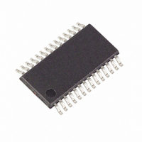
MAXQ3108-FFN+ Maxim Integrated Products, MAXQ3108-FFN+ Datasheet - Page 22

MAXQ3108-FFN+
Manufacturer Part Number
MAXQ3108-FFN+
Description
IC MCU DUAL-CORE 16BIT 28-TSSOP
Manufacturer
Maxim Integrated Products
Series
MAXQ™r
Datasheet
1.MAXQ3108-FFN.pdf
(64 pages)
Specifications of MAXQ3108-FFN+
Core Processor
RISC
Core Size
16-Bit
Speed
10MHz
Connectivity
I²C, SPI, UART/USART
Peripherals
POR, PWM, WDT
Number Of I /o
21
Program Memory Size
64KB (32K x 16)
Program Memory Type
FLASH
Ram Size
11K x 8
Voltage - Supply (vcc/vdd)
1.8 V ~ 3.6 V
Oscillator Type
External
Operating Temperature
-40°C ~ 85°C
Package / Case
28-TSSOP
Processor Series
MAXQ
Core
RISC
Data Bus Width
16 bit
Data Ram Size
2 KB
Interface Type
I2C, JTAG, SPI
Maximum Clock Frequency
10 MHz
Number Of Programmable I/os
22
Number Of Timers
2
Operating Supply Voltage
3.6 V
Maximum Operating Temperature
+ 85 C
Mounting Style
SMD/SMT
Minimum Operating Temperature
- 40 C
Lead Free Status / RoHS Status
Lead free / RoHS Compliant
Eeprom Size
-
Data Converters
-
Lead Free Status / Rohs Status
Lead free / RoHS Compliant
Low-Power, Dual-Core Microcontroller
22
MSTC.[5:4]: CCSL[1:0]
MSTC.[7:6]: Reserved
PO0 (00h, 01h)
Initialization:
Read/Write Access:
PO0.[7:0]:
PO1 (01h, 01h)
Initialization:
Read/Write Access:
PO1.[6:0]:
PO1.7: Reserved
______________________________________________________________________________________
Clock Correction Hardware Selection Bits 1:0. These bits are used to enable and assign the
clock measurement hardware to one of the three Manchester decoders. When these bits are 11b,
the clock measurement utility is disabled. Writing these bits to any other state enables one clock
measurement interval. When the clock measurement interval is enabled, the ADCC output register
is cleared to 0000h to indicate a busy (measuring) condition. No hardware protection is in place to
prevent attempts to measure a disabled decoder, which would result in seeing a persistent busy
(ADCC = 0000h) condition. The table below summarizes the measurement options.
Separate physical implementations of these two control bits exist for the UserCore and the
DSPCore. The ENDSP bit controls which bits are used to control the clock correction measurement
hardware. When ENDSP = 0, the UserCore CCSL[1:0] bits control the hardware. When ENDSP = 1,
the DSPCore CCSL[1:0] bits control the hardware. The bits not being used by the hardware are still
write accessible but have no effect on the hardware. Once a clock measurement is requested, a
second request should not be issued from the other core. There is no need for hardware protection
against this possibility; the ADCC register can be polled to ascertain the busy status.
Reserved. Reads return 0.
Port 0 Output Register (8-Bit Register)
This register is set to 0FFh on all forms of reset.
Unrestricted read/write.
Port 0 Output Register Bits 7:0. The PO0 register stores output data for port 0 when it is defined as
an output port and controls whether the internal weak p-channel pullup transistor is
enabled/disabled if a port pin is defined as an input. The contents of this register can be modified
by a write access. Reading from the register returns the contents of the register. Changing the
direction of port 0 does not change the data contents of the register.
Port 1 Output Register (8-Bit Register)
This register is set to 07Fh on all forms of reset.
Unrestricted read/write.
Port 1 Output Register Bits 6:0. The PO1 register stores output data for port 1 when it is defined as
an output port and controls whether the internal weak p-channel pullup transistor is
enabled/disabled if a port pin is defined as an input. The contents of this register can be modified
by a write access. Reading from the register returns the contents of the register. Changing the
direction of port 1 does not change the data contents of the register.
Special note about P1.6: The RST input function remains enabled on P1.6 unless it is explicitly
disabled (RSTD = 1). This means that the ports control bits (PD, PO) can be used to generate a
reset (e.g., by driving the pin low).
Reserved. Reads return 0.
Special Function Register Bit Descriptions (continued)
CCSL[1:0]
00b
01b
10b
11b
CLOCK MEASUREMENT (SYNC BIT
FREQUENCY)
Decoder 0
Decoder 1
Decoder 2
Disabled


