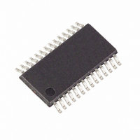
MAXQ3108-FFN+ Maxim Integrated Products, MAXQ3108-FFN+ Datasheet - Page 36

MAXQ3108-FFN+
Manufacturer Part Number
MAXQ3108-FFN+
Description
IC MCU DUAL-CORE 16BIT 28-TSSOP
Manufacturer
Maxim Integrated Products
Series
MAXQ™r
Datasheet
1.MAXQ3108-FFN.pdf
(64 pages)
Specifications of MAXQ3108-FFN+
Core Processor
RISC
Core Size
16-Bit
Speed
10MHz
Connectivity
I²C, SPI, UART/USART
Peripherals
POR, PWM, WDT
Number Of I /o
21
Program Memory Size
64KB (32K x 16)
Program Memory Type
FLASH
Ram Size
11K x 8
Voltage - Supply (vcc/vdd)
1.8 V ~ 3.6 V
Oscillator Type
External
Operating Temperature
-40°C ~ 85°C
Package / Case
28-TSSOP
Processor Series
MAXQ
Core
RISC
Data Bus Width
16 bit
Data Ram Size
2 KB
Interface Type
I2C, JTAG, SPI
Maximum Clock Frequency
10 MHz
Number Of Programmable I/os
22
Number Of Timers
2
Operating Supply Voltage
3.6 V
Maximum Operating Temperature
+ 85 C
Mounting Style
SMD/SMT
Minimum Operating Temperature
- 40 C
Lead Free Status / RoHS Status
Lead free / RoHS Compliant
Eeprom Size
-
Data Converters
-
Lead Free Status / Rohs Status
Lead free / RoHS Compliant
Low-Power, Dual-Core Microcontroller
36
SMD0.7: EPWM
PR0 (09h, 02h)
Initialization:
Read/Write Access:
PR0.[15:0]:
PD2 (0Ah, 02h)
Initialization:
Read/Write Access:
PD2.[6:0]:
PD2.7: Reserved
T2CNB (0Bh, 02h)
Initialization:
Read/Write Access:
T2CNB.0: T2CL
T2CNB.1: TCC2
T2CNB.2: TF2L
T2CNB.3: TF2
T2CNB.4: Reserved
T2CNB.5: T2POL1
______________________________________________________________________________________
Enable TXD PWM Output Function. Setting this bit to a 1 enables the output of the logical function
selected by the OFS bit to be output on the TXD0 pin for the asynchronous UART transmit modes
(i.e., modes 1, 2, and 3). Note that the PWM function is not possible for UART mode 0 and this bit
has no effect during UART mode 0 operation. When this bit is cleared to 0, the OFS bit is
meaningless and the normal TXD0 pin controls and behavior apply.
Phase Register 0
The phase register is cleared to 0000h on all forms of reset.
Unrestricted read/write.
Phase Register 0 15:0. This register is used to load and read the 16-bit value in the phase register
that determines the baud rate for the serial port 0.
Port 2 Direction Register
This register is cleared to 00h on all forms of reset.
Unrestricted read/write.
Port 2 Direction Register Bits 6:0. PD2 is used to determine the direction of the port 2 function. The
port pins are independently controlled by their direction bit. When a bit is set to 1, its corresponding
pin is used as an output; data in the PO register is driven on the pin. When a bit is cleared to 0, its
corresponding pin is used as an input, and allows an external signal to drive the pin. Note that each
port pin has a weak pullup circuit when functioning as an input and the p-channel pullup transistor is
controlled by its respective PO bits. If the PO bit is set to 1, the weak pullup is on; if the PO bit is
cleared to 0, the weak pullup is off and forces the port pin into three-state.
Reserved. Reads return 0.
Timer 2 Control Register B
This register is cleared to 00h on all forms of reset.
Unrestricted read/write.
Timer 2 Low Compare Flag. This flag is meaningful only for the dual 8-bit mode of operation (T2MD
= 1) and becomes set only when a compare match occurs between T2CL and T2L. Timer 2 low
does not have an associated capture function.
Timer 2 Capture/Compare Flag. This flag is set on any compare match between the Timer 2 value
and compare register (T2V = T2C or T2H = T2CH, respectively, for 16-bit and 8-bit compare modes)
or when a capture event is initiated by an external edge.
Timer 2 Low Overflow Flag. This flag is meaningful only when in the dual 8-bit mode of operation
(T2MD = 1) and becomes set whenever there is an overflow of the T2L 8-bit timer.
Timer 2 Overflow Flag. This flag becomes set anytime there is an overflow of the full 16-bit T2
timer/counter (when T2MD = 0) or an overflow of the 8-bit T2H timer/counter when the dual 8-bit
mode of operation is selected (T2MD = 1).
Reserved. Reads return 0.
Timer 2 Polarity Select 1. When the T2B output is enabled (T2OE1 = 1), this bit selects the starting
logic level for the alternate pin output. The output that is driven on the T2PB pin can be derived
from the 16-bit timer 2 or the 8-bit timer (T2L) depending upon whether operating in the 16-bit mode
or the dual 8-bit mode. The T2POL1 bit can be modified any time, but takes effect on the external
pin when T2OE1 is changed from 0 to 1.
Special Function Register Bit Descriptions (continued)


