MAXQ3108-FFN+ Maxim Integrated Products, MAXQ3108-FFN+ Datasheet - Page 48
MAXQ3108-FFN+
Manufacturer Part Number
MAXQ3108-FFN+
Description
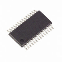
IC MCU DUAL-CORE 16BIT 28-TSSOP
Manufacturer
Maxim Integrated Products
Series
MAXQ™r
Datasheet
1.MAXQ3108-FFN.pdf
(64 pages)
Specifications of MAXQ3108-FFN+
Core Processor
RISC
Core Size
16-Bit
Speed
10MHz
Connectivity
I²C, SPI, UART/USART
Peripherals
POR, PWM, WDT
Number Of I /o
21
Program Memory Size
64KB (32K x 16)
Program Memory Type
FLASH
Ram Size
11K x 8
Voltage - Supply (vcc/vdd)
1.8 V ~ 3.6 V
Oscillator Type
External
Operating Temperature
-40°C ~ 85°C
Package / Case
28-TSSOP
Processor Series
MAXQ
Core
RISC
Data Bus Width
16 bit
Data Ram Size
2 KB
Interface Type
I2C, JTAG, SPI
Maximum Clock Frequency
10 MHz
Number Of Programmable I/os
22
Number Of Timers
2
Operating Supply Voltage
3.6 V
Maximum Operating Temperature
+ 85 C
Mounting Style
SMD/SMT
Minimum Operating Temperature
- 40 C
Lead Free Status / RoHS Status
Lead free / RoHS Compliant
Eeprom Size
-
Data Converters
-
Lead Free Status / Rohs Status
Lead free / RoHS Compliant


Low-Power, Dual-Core Microcontroller
48
I2CCN (0Ch, 04h)
Initialization:
Read/Write Access:
I2CCN.0: I2CEN
I2CCN.1: I2CMST
I2CCN.2: I2CMODE
I2CCN.3: Reserved
I2CCN.4: I2CSTRS
I2CCN.5: I2CACK
I2CCN.6: I2CSTART
______________________________________________________________________________________
I
This register is cleared to 0000h on all forms of reset. The I2CSTART and I2CSTOP bits are reset to
0 when I2CMST = 0 or when I2CEN = 0. I2CSTART and I2CSTOP are mutually exclusive
operations. User software can only set one of these bits at any given time. I2CRST is reset to 0
when I2CEN = 0.
Unrestricted read. Unrestricted write access when I2CBUSY = 0. Writes to I2CMST, I2CMODE are
ignored when I2CBUSY = 1. Writes to I2CEN are normally disabled when I2CBUSY = 1. However,
when I2CRST = 1, I2CEN can be written to even when I2CBUSY = 1. Writes to I2CACK are ignored
when I2CRST = 1.
I
enabled. When cleared to 0, the I
I
module. When the I2CMST bit is set to 1, the I 2 C operates as a master. When the I2CMST is
cleared to 0, the I
the I
receives a general call (I2CGCI = 1).
I
master. When the I2CMODE bit is set to 1, the master is operating in receiver mode (reading from
slave). When the I2CMODE bit is cleared to 0, the master is operating in transmitter mode (writing
to slave). Note that software writing to this bit is prohibited in slave mode. When operating in
master mode, software configures this bit to the desired direction of data transfer. When operating
in slave mode, the direction of data transfer is determined by the R/W bit received during the
address stage and this bit reflects the actual R/W bit value in the current transfer and is set by
hardware. Software writing to this bit in slave mode is ignored.
Reserved. Do not write a 1 to this location. Functionally, this is the I2CEA bit, however, there are
problems with the I
I
8th clock cycle. Clearing this bit to 0 enables clock stretching after the falling edge of the 9th
clock cycle. This bit has no effect when clock stretching is disabled (I2CSTREN = 0).
I
acting as a receiver. Setting this bit to 1 generates a NACK (leaving SDA high). Clearing the
I2CACK bit to 0 generates an ACK (pulling SDA LOW) during the acknowledgement cycle. This bit
retains its value unless changed by software or hardware. When an I
(I2CRST = 1), this bit is set to 1 by hardware and software writes to this bit are ignored when
I2CRST = 1.
I
or generates a repeated START condition during a transfer where the I
master. This bit is automatically self-cleared to 0 after the START condition has been generated. If
the I
In master mode, setting this bit could also start the timeout timer if enabled. If the timeout timer
expires before the START condition can be generated, a timeout interrupt is generated to the CPU if
enabled. The I2CSTART bit is also cleared to 0 by the timeout event.
Note that this bit has no effect when the I
to 0 when I2CMST = 0 or I2CEN = 0. Also, the I2CSTART and I2CSTOP are mutually exclusive. If
both bits are set at the same time, it is considered as an invalid operation and the I
ignores the request and resets both bits to 0. Setting the I2CSTART bit to 1 while I2CSTOP = 1 is an
invalid operation and is ignored, leaving the I2CSTART bit cleared to 0.
2
2
2
2
2
2
2
C START Enable. Setting this bit automatically generates a START condition when the bus is free
C Control Register (16-Bit Register)
C Enable. This bit enables the I
C Master Mode Enable. The I2CMST bit functions as a master mode enable bit for the I
C Transfer Mode. The transfer mode bit selects the direction of data transfer with respect to the
C Clock Stretch Select. Setting this bit to 1 enables clock stretching after the falling edge of the
C Data Acknowledge Bit. This bit selects the acknowledge bit returned by the I
Special Function Register Bit Descriptions (continued)
2
2
C START interrupt is enabled, a START condition generates an interrupt to the CPU.
C controller receives a slave address match (I2CAMI = 1), loses arbitration (I2CALI = 1), or
2
C module operates in slave mode. This bit is automatically cleared whenever
2
C extended addressing mode.
2
2
C function is disabled.
C function. When set to 1, the I
2
C is operating in slave mode (I2CMST = 0) and is reset
2
C communication unit is
2
2
C module is operating as the
C abort is in progress
2
C controller while
2
C controller
2
C
Related parts for MAXQ3108-FFN+
Image
Part Number
Description
Manufacturer
Datasheet
Request
R

Part Number:
Description:
Dual-Core Microcontroller
Manufacturer:
Maxim Integrated Products
Datasheet:

Part Number:
Description:
Low-power, Dual-core Microcontroller
Manufacturer:
Maxim Integrated Products, Inc.
Datasheet:
Part Number:
Description:
MAX7528KCWPMaxim Integrated Products [CMOS Dual 8-Bit Buffered Multiplying DACs]
Manufacturer:
Maxim Integrated Products
Datasheet:
Part Number:
Description:
Single +5V, fully integrated, 1.25Gbps laser diode driver.
Manufacturer:
Maxim Integrated Products
Datasheet:
Part Number:
Description:
Single +5V, fully integrated, 155Mbps laser diode driver.
Manufacturer:
Maxim Integrated Products
Datasheet:
Part Number:
Description:
VRD11/VRD10, K8 Rev F 2/3/4-Phase PWM Controllers with Integrated Dual MOSFET Drivers
Manufacturer:
Maxim Integrated Products
Datasheet:
Part Number:
Description:
Highly Integrated Level 2 SMBus Battery Chargers
Manufacturer:
Maxim Integrated Products
Datasheet:
Part Number:
Description:
Current Monitor and Accumulator with Integrated Sense Resistor; ; Temperature Range: -40°C to +85°C
Manufacturer:
Maxim Integrated Products
Part Number:
Description:
TSSOP 14/A°/RS-485 Transceivers with Integrated 100O/120O Termination Resis
Manufacturer:
Maxim Integrated Products
Part Number:
Description:
TSSOP 14/A°/RS-485 Transceivers with Integrated 100O/120O Termination Resis
Manufacturer:
Maxim Integrated Products
Part Number:
Description:
QFN 16/A°/AC-DC and DC-DC Peak-Current-Mode Converters with Integrated Step
Manufacturer:
Maxim Integrated Products
Part Number:
Description:
TDFN/A/65V, 1A, 600KHZ, SYNCHRONOUS STEP-DOWN REGULATOR WITH INTEGRATED SWI
Manufacturer:
Maxim Integrated Products
Part Number:
Description:
Integrated Temperature Controller f
Manufacturer:
Maxim Integrated Products
Part Number:
Description:
SOT23-6/I°/45MHz to 650MHz, Integrated IF VCOs with Differential Output
Manufacturer:
Maxim Integrated Products
Part Number:
Description:
SOT23-6/I°/45MHz to 650MHz, Integrated IF VCOs with Differential Output
Manufacturer:
Maxim Integrated Products