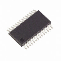
MAXQ3108-FFN+ Maxim Integrated Products, MAXQ3108-FFN+ Datasheet - Page 53

MAXQ3108-FFN+
Manufacturer Part Number
MAXQ3108-FFN+
Description
IC MCU DUAL-CORE 16BIT 28-TSSOP
Manufacturer
Maxim Integrated Products
Series
MAXQ™r
Datasheet
1.MAXQ3108-FFN.pdf
(64 pages)
Specifications of MAXQ3108-FFN+
Core Processor
RISC
Core Size
16-Bit
Speed
10MHz
Connectivity
I²C, SPI, UART/USART
Peripherals
POR, PWM, WDT
Number Of I /o
21
Program Memory Size
64KB (32K x 16)
Program Memory Type
FLASH
Ram Size
11K x 8
Voltage - Supply (vcc/vdd)
1.8 V ~ 3.6 V
Oscillator Type
External
Operating Temperature
-40°C ~ 85°C
Package / Case
28-TSSOP
Processor Series
MAXQ
Core
RISC
Data Bus Width
16 bit
Data Ram Size
2 KB
Interface Type
I2C, JTAG, SPI
Maximum Clock Frequency
10 MHz
Number Of Programmable I/os
22
Number Of Timers
2
Operating Supply Voltage
3.6 V
Maximum Operating Temperature
+ 85 C
Mounting Style
SMD/SMT
Minimum Operating Temperature
- 40 C
Lead Free Status / RoHS Status
Lead free / RoHS Compliant
Eeprom Size
-
Data Converters
-
Lead Free Status / Rohs Status
Lead free / RoHS Compliant
Table 6. MAXQ3108 Clock Divisors
modes. The two power-management modes reduce
speed and power consumption by either internally
dividing the clock signal by 256 or using the 32kHz
clock directly. The stop mode stops all internal clocks
(with the exception of the 32kHz crystal amplifier)
resulting in a static condition and providing the lowest
power state.
The power supervisor monitors the V
power is first applied to the device and generates a
power-on reset when the voltage reaches an accept-
able level, and following the 65,536 FLL cycle power-up
period.
The power-on reset initializes the processor and allows
program execution at the reset vector location of
8000h. The power-on reset flag, POR, is set to logic 1 to
indicate a power-on reset has occurred; the POR flag
can only be cleared by software.
Power-management mode (PMM) allows application
software to dynamically match operating frequency with
the need for lower operating power when full process-
ing throughput is not required. When power-manage-
ment mode 1 (PMM1) is used, the system clock is
divided by 256, resulting in a user core clock rate of
19.584kHz. When power-management mode 2 (PMM2)
is used, the system clock is driven directly by the
32,768Hz clock source resulting in a user core clock of
16.384kHz.
PMM reduces operating power by minimizing power
loss due to CMOS switching transients. PMM is invoked
by setting the PMM enable bit (PMME). The PMME bit
defaults to 0 on all forms of reset.
When the system is operated in PMM2 mode, the high-
frequency clock is disabled unless the switchback is
active or the DSPCore is enabled. Refer to the PMME
bit description in the MAXQ Family User’s Guide for
more information.
PMME
0
0
0
0
1
1
1
1
______________________________________________________________________________________
Low-Power, Dual-Core Microcontroller
CD[1:0]
00
01
10
11
00
01
10
11
Power-Management Mode
DD
level when
Reserved (256)
Reserved (256)
DIVIDE RATIO
1 (default)
256
2
4
8
1
The switchback feature allows low-power operation
associated with PMM, but maintains quick response to
events that require full processing capacity. The switch-
back function is enabled by setting the SWB bit to logic
1. When operating in a PMM mode and the SWB bit is
enabled, the system restores the clock settings that
were active when PMM was invoked whenever the sys-
tem detects a qualified event.
The automatic switchback is only enabled when PMM is
in use. Switchback to the high-frequency clock occurs
whenever any of these conditions occur:
• Detection of a selected edge transition on any of the
• UART activity:
• SPI activity:
• Time-of-day alarm or subsecond alarm from the RTC
• I
• SVM interrupt if enabled (SVMIE = 1).
• Changing the value of ADCONV from 0 to 1.
• Active debug mode is entered either by breakpoint
external interrupts when the respective pin has inter-
rupts enabled.
• When the serial port is enabled to receive data and
• After a write access to the SBUF register.
• SPIB is written in master mode (STBY = 1).
• The SSEL signal is asserted in slave mode.
when enabled.
• Start interrupt when enabled (I2CSRIE = 1).
• A write to the I2CSTART bit when the I
match or issuance of the debug command from
background mode.
2
C activity:
a transition occurs on the receive input pin (for
mode 1, 2, and 3).
is in master mode (I2CMST = 1).
CLOCK SOURCE
FLLSL
FLLSL
FLLSL
FLLSL
FLLSL
FLLSL
FLLSL
CX1
2
Switchback
C controller
53


