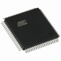
AT89C5132-ROTIL Atmel, AT89C5132-ROTIL Datasheet - Page 111

AT89C5132-ROTIL
Manufacturer Part Number
AT89C5132-ROTIL
Description
IC 8051 MCU FLASH 64K USB 80TQFP
Manufacturer
Atmel
Series
AT89C513xr
Datasheets
1.AT89C5132-ROTUL.pdf
(182 pages)
2.AT89C5132-ROTUL.pdf
(38 pages)
3.AT89C5132-ROTIL.pdf
(33 pages)
Specifications of AT89C5132-ROTIL
Core Processor
C52X2
Core Size
8-Bit
Speed
20MHz
Connectivity
IDE/ATAPI, I²C, MMC, PCM, SPI, UART/USART, USB
Peripherals
I²S, POR, WDT
Number Of I /o
44
Program Memory Size
64KB (64K x 8)
Program Memory Type
FLASH
Eeprom Size
4K x 8
Ram Size
2.25K x 8
Voltage - Supply (vcc/vdd)
2.7 V ~ 3.3 V
Data Converters
A/D 2x10b
Oscillator Type
Internal
Operating Temperature
-40°C ~ 85°C
Package / Case
80-TQFP, 80-VQFP
Lead Free Status / RoHS Status
Contains lead / RoHS non-compliant
Available stocks
Company
Part Number
Manufacturer
Quantity
Price
- Current page: 111 of 182
- Download datasheet (2Mb)
18.4
18.4.0.1
18.4.0.2
18.4.1
4173E–USB–09/07
Asynchronous Modes (Modes 1, 2 and 3)
Transmission
(Modes 1, 2 and 3)
Mode 1
Modes 2 and 3
The Serial Port has one 8-bit and two 9-bit asynchronous modes of operation. Figure 18-8
shows the Serial Port block diagram in asynchronous modes.
Figure 18-8. Serial I/O Port Block Diagram (Modes 1, 2 and 3)
Mode 1 is a full-duplex, asynchronous mode. The data frame (see Figure 18-9) consists of 10
Bits: one start, eight data Bits and one stop bit. Serial data is transmitted on the TXD pin and
received on the RXD pin. When data is received, the stop bit is read in the RB8 bit in SCON
register.
Figure 18-9. Data Frame Format (Mode 1)
Modes 2 and 3 are full-duplex, asynchronous modes. The data frame (see Figure 18-10) con-
sists of 11 Bits: one start bit, eight data Bits (transmitted and received LSB first), one
programmable ninth data bit and one stop bit. Serial data is transmitted on the TXD pin and
received on the RXD pin. On receive, the ninth bit is read from RB8 bit in SCON register. On
transmit, the ninth data bit is written to TB8 bit in SCON register. Alternatively, the ninth bit can
be used as a command/data flag.
Figure 18-10. Data Frame Format (Modes 2 and 3)
To initiate a transmission, write to SCON register, setting SM0 and SM1 Bits according to
Table 89, and setting the ninth bit by writing to TB8 bit. Then, writing the byte to be transmitted to
SBUF register starts the transmission.
Mode 1
CLOCK
CLOCK
CLOCK
IBRG
PER
T1
Start bit
Start bit
SCON.4
SM2
D0
SCON.6
M3 M2 M1 M0
SM1
Mode Decoder
Mode & Clock
D0
Controller
D1
SCON.1
TI
D1
SCON.7
D2
SM0
SCON.0
D2
RI
D3
9-bit data
D3
8-bit data
D4
D4
D5
D5
SBUF Tx SR
SBUF Rx
D6
Rx SR
SCON.3
TB8
D6
D7
AT89C5132
D7
D8
SCON.2
Stop bit
RB8
Stop bit
TXD
RXD
111
Related parts for AT89C5132-ROTIL
Image
Part Number
Description
Manufacturer
Datasheet
Request
R

Part Number:
Description:
Manufacturer:
Atmel Corporation
Datasheet:

Part Number:
Description:
MCU 8051 FLASH USB 80TQFP
Manufacturer:
Atmel
Datasheet:

Part Number:
Description:
DEV KIT FOR AVR/AVR32
Manufacturer:
Atmel
Datasheet:

Part Number:
Description:
INTERVAL AND WIPE/WASH WIPER CONTROL IC WITH DELAY
Manufacturer:
ATMEL Corporation
Datasheet:

Part Number:
Description:
Low-Voltage Voice-Switched IC for Hands-Free Operation
Manufacturer:
ATMEL Corporation
Datasheet:

Part Number:
Description:
MONOLITHIC INTEGRATED FEATUREPHONE CIRCUIT
Manufacturer:
ATMEL Corporation
Datasheet:

Part Number:
Description:
AM-FM Receiver IC U4255BM-M
Manufacturer:
ATMEL Corporation
Datasheet:

Part Number:
Description:
Monolithic Integrated Feature Phone Circuit
Manufacturer:
ATMEL Corporation
Datasheet:

Part Number:
Description:
Multistandard Video-IF and Quasi Parallel Sound Processing
Manufacturer:
ATMEL Corporation
Datasheet:

Part Number:
Description:
High-performance EE PLD
Manufacturer:
ATMEL Corporation
Datasheet:

Part Number:
Description:
8-bit Flash Microcontroller
Manufacturer:
ATMEL Corporation
Datasheet:


