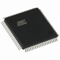
AT89C5132-ROTIL Atmel, AT89C5132-ROTIL Datasheet - Page 112

AT89C5132-ROTIL
Manufacturer Part Number
AT89C5132-ROTIL
Description
IC 8051 MCU FLASH 64K USB 80TQFP
Manufacturer
Atmel
Series
AT89C513xr
Datasheets
1.AT89C5132-ROTUL.pdf
(182 pages)
2.AT89C5132-ROTUL.pdf
(38 pages)
3.AT89C5132-ROTIL.pdf
(33 pages)
Specifications of AT89C5132-ROTIL
Core Processor
C52X2
Core Size
8-Bit
Speed
20MHz
Connectivity
IDE/ATAPI, I²C, MMC, PCM, SPI, UART/USART, USB
Peripherals
I²S, POR, WDT
Number Of I /o
44
Program Memory Size
64KB (64K x 8)
Program Memory Type
FLASH
Eeprom Size
4K x 8
Ram Size
2.25K x 8
Voltage - Supply (vcc/vdd)
2.7 V ~ 3.3 V
Data Converters
A/D 2x10b
Oscillator Type
Internal
Operating Temperature
-40°C ~ 85°C
Package / Case
80-TQFP, 80-VQFP
Lead Free Status / RoHS Status
Contains lead / RoHS non-compliant
Available stocks
Company
Part Number
Manufacturer
Quantity
Price
- Current page: 112 of 182
- Download datasheet (2Mb)
18.4.2
18.4.3
18.4.4
112
AT89C5132
Reception
(Modes 1, 2 and 3)
Framing Error Detection
(Modes 1, 2 and 3)
Baud Rate Selection (Modes 1 and 3)
To prepare for reception, write to SCON register, setting SM0 and SM1 Bits according to
Table 89, and set the REN bit. The actual reception is then initiated by a detected high-to-low
transition on the RXD pin.
Framing error detection is provided for the three asynchronous modes. To enable the framing bit
error detection feature, set SMOD0 bit in PCON register as shown in Figure 18-11.
When this feature is enabled, the receiver checks each incoming data frame for a valid stop bit.
An invalid stop bit may result from noise on the serial lines or from simultaneous transmission by
two devices. If a valid stop bit is not found, the software sets FE bit in SCON register.
Software may examine FE bit after each reception to check for data errors. Once set, only soft-
ware or a chip reset clears FE bit. Subsequently received frames with valid stop Bits cannot
clear FE bit. When the framing error detection feature is enabled, RI rises on stop bit instead of
the last data bit as detailed in Figure 18-17.
Figure 18-11. Framing Error Block Diagram
In modes 1 and 3, the Baud Rate is derived either from the Timer 1 or the Internal Baud Rate
Generator and allows different baud rate in reception and transmission.
As shown in Figure 18-12, the selection is done using RBCK and TBCK Bits in BDRCON
register.
Figure 18-13 gives the baud rate calculation formulas for each baud rate source. Table 90
details Internal Baud Rate Generator configuration for different peripheral clock frequencies and
gives baud rates closer to the standard baud rates.
Figure 18-12. Baud Rate Source Selection (Modes 1 and 3)
CLOCK
CLOCK
IBRG
T1
BDRCON.2
RBCK
Framing Error
0
1
Controller
÷ 16
FE
To Serial
Rx Port
SM0
SMOD0
PCON.6
CLOCK
CLOCK
1
0
IBRG
T1
SM0/FE
BDRCON.3
SCON.7
TBCK
0
1
÷ 16
4173E–USB–09/07
To Serial
Tx Port
Related parts for AT89C5132-ROTIL
Image
Part Number
Description
Manufacturer
Datasheet
Request
R

Part Number:
Description:
Manufacturer:
Atmel Corporation
Datasheet:

Part Number:
Description:
MCU 8051 FLASH USB 80TQFP
Manufacturer:
Atmel
Datasheet:

Part Number:
Description:
DEV KIT FOR AVR/AVR32
Manufacturer:
Atmel
Datasheet:

Part Number:
Description:
INTERVAL AND WIPE/WASH WIPER CONTROL IC WITH DELAY
Manufacturer:
ATMEL Corporation
Datasheet:

Part Number:
Description:
Low-Voltage Voice-Switched IC for Hands-Free Operation
Manufacturer:
ATMEL Corporation
Datasheet:

Part Number:
Description:
MONOLITHIC INTEGRATED FEATUREPHONE CIRCUIT
Manufacturer:
ATMEL Corporation
Datasheet:

Part Number:
Description:
AM-FM Receiver IC U4255BM-M
Manufacturer:
ATMEL Corporation
Datasheet:

Part Number:
Description:
Monolithic Integrated Feature Phone Circuit
Manufacturer:
ATMEL Corporation
Datasheet:

Part Number:
Description:
Multistandard Video-IF and Quasi Parallel Sound Processing
Manufacturer:
ATMEL Corporation
Datasheet:

Part Number:
Description:
High-performance EE PLD
Manufacturer:
ATMEL Corporation
Datasheet:

Part Number:
Description:
8-bit Flash Microcontroller
Manufacturer:
ATMEL Corporation
Datasheet:


