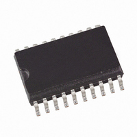
ATAM893T-TKS Atmel, ATAM893T-TKS Datasheet - Page 24

ATAM893T-TKS
Manufacturer Part Number
ATAM893T-TKS
Description
IC MON TIRE-PRESS ATARX9X SER
Manufacturer
Atmel
Series
MARC4r
Datasheet
1.ATAM893T-TKS.pdf
(98 pages)
Specifications of ATAM893T-TKS
Core Processor
MARC4
Core Size
4-Bit
Speed
4MHz
Connectivity
SSI (2-Wire, 3 Wire)
Peripherals
Brown-out Detect/Reset, POR, PWM, WDT
Number Of I /o
16
Program Memory Size
4KB (4K x 8)
Program Memory Type
EEPROM
Eeprom Size
64 x 16
Ram Size
256 x 4
Voltage - Supply (vcc/vdd)
1.8 V ~ 6.5 V
Oscillator Type
Internal
Operating Temperature
-40°C ~ 125°C
Package / Case
20-SOIC (5.3mm Width), 20-SO, 20-SOEIAJ
Lead Free Status / RoHS Status
Contains lead / RoHS non-compliant
Data Converters
-
5.2
5.2.1
24
Bi-directional Ports
ATAM893-D
Bi-directional Port 1
With the exception of Port 1 and Port 6, all other ports (2, 4 and 5) are 4 bits wide. Port 1 and
Port 6 have a data width of 2 bits (bit 0 and bit 3). All ports may be used for data input or output.
All ports are equipped with Schmitt trigger inputs and a variety of mask options for open drain,
open source, full complementary outputs, pull-up and pull-down transistors. All Port Data Regis-
ters (PxDAT) are I/O mapped to the primary address register of the respective port address and
the Port Control Register (PxCR), to the corresponding auxiliary register.
There are five different directional ports available:
Port 1
Port 2
Port 5
Port 4
Port 6
In Port 1 the data direction register is not independently software programmable, the direction of
the complete port being switched automatically when an I/O instruction occurs (see
on page
instruction. The data written to a port will be stored into the output data latches and appears
immediately at the port pin following the OUT instruction. After RESET all output latches are set
to '1' and the port is switched to input mode. An IN instruction reads the condition of the associ-
ated pins.
Note:
Care must be taken when switching the bi-directional port from output to input. The capacitive pin
loading at this port in conjunction with the high resistance pull-ups may cause the CPU to read the
contents of the output data register rather than the external input state. To avoid this, one of the
following programming techniques should be used:
Use two IN-instructions and DROP the first data nibble. The first IN switches the port from output
to input and the DROP removes the first invalid nibble. The second IN reads the valid pin state.
Use an OUT-instruction followed by an IN-instruction. Via the OUT-instruction, the capacitive load
is charged or discharged depending on the optional pull-up/pull-down configuration. Write a '1' for
pins with pull-up resistors and a '0' for pins with pull-down resistors.
25). The port is switched to output mode via an OUT instruction and to input via an IN
2-bit wide bi-directional ports with automatic full bus width direction switching
4-bit wide bit-wise-programmable I/O port
4-bit wide bit-wise-programmable bi-directional port with optional strong pull-ups
and programmable interrupt logic
4-bit wide bit-wise-programmable bi-directional port also provides the I/O interface
to Timer 2, SSI, voltage monitor input and external interrupt input
2-bit wide bit-wise-programmable bi-directional port also provides the I/O interface
to Timer 3 and external interrupt input
4680C–4BMCU–01/05
Figure 5-2


