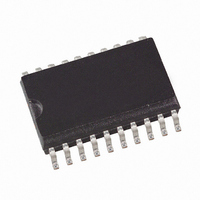
ATAM893T-TKS Atmel, ATAM893T-TKS Datasheet - Page 51

ATAM893T-TKS
Manufacturer Part Number
ATAM893T-TKS
Description
IC MON TIRE-PRESS ATARX9X SER
Manufacturer
Atmel
Series
MARC4r
Datasheet
1.ATAM893T-TKS.pdf
(98 pages)
Specifications of ATAM893T-TKS
Core Processor
MARC4
Core Size
4-Bit
Speed
4MHz
Connectivity
SSI (2-Wire, 3 Wire)
Peripherals
Brown-out Detect/Reset, POR, PWM, WDT
Number Of I /o
16
Program Memory Size
4KB (4K x 8)
Program Memory Type
EEPROM
Eeprom Size
64 x 16
Ram Size
256 x 4
Voltage - Supply (vcc/vdd)
1.8 V ~ 6.5 V
Oscillator Type
Internal
Operating Temperature
-40°C ~ 125°C
Package / Case
20-SOIC (5.3mm Width), 20-SO, 20-SOEIAJ
Lead Free Status / RoHS Status
Contains lead / RoHS non-compliant
Data Converters
-
5.3.3.3
4680C–4BMCU–01/05
Timer 3 Modulator/Demodulator Modes
Timer 3 – Mode 3:
The counter is driven by an internal or external (T3I) clock source. The output toggle signal of
Timer 2 resets the counter. The counter value before the reset is saved in the capture register. If
single-action mode is activated for one or both compare registers, the trigger signal restarts the
single actions. This mode can be used for frequency measurements or as event counter with
time gate (see section “Combination Mode 10”).
Figure 5-30. Event Counter with Time Gate
Timer 3 – Mode 4:
The timer runs as timer/counter in mode 1, but its output T3O is used as output for the Timer 2
output signal.
Timer 3 – Mode 5:
The Timer 3 runs as timer/counter in mode 2, but its output T3O is used as output for the Timer
2 output signal.
Timer 3 – Mode 6:
The Timer 3 counter is driven by an internal or external clock source. Its compare- and compare
mode registers must be programmed to generate the carrier frequency via the output toggle flip-
flop. The output toggle flip-flop of Timer 2 is used to enable or disable the Timer 3 output. Timer
2 can be driven by the toggle output signal of Timer 3 or any other clock source (see section
“Combination Mode 11”).
Timer 3 – Mode 7:
The Timer 3 counter is driven by an internal or external clock source. Its compare- and compare
mode registers must be programmed to generate the carrier frequency via the output toggle flip-
flop. The output (SO) of the SSI is used to enable or disable the Timer 3 output. The SSI should
be supplied with the toggle signal of Timer 2 (see section “Combination Mode 12”).
Counter 3
Register
T3CP-
TOG2
T3R
T3I
0 0 1 2 3 4 5 6 7 8 910
Timer/Counter, Internal Trigger Restart and Internal Capture
(with TOG2)
Timer/Counter
Timer/Counter, External Trigger Restart and External Capture
(with T3I Input)
Carrier Frequency Burst Modulation Controlled by Timer 2 Output
Toggle Flip–Flop (M2)
Carrier Frequency Burst Modulation Controlled by SSI Internal
Output (SO)
Capture value = 0
11
0 1
2
Capture value = 11
3
ATAM893-D
4
Capture value = 4
0 1
2
51


