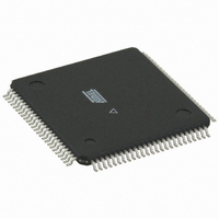
ATMEGA6490-16AI Atmel, ATMEGA6490-16AI Datasheet - Page 203

ATMEGA6490-16AI
Manufacturer Part Number
ATMEGA6490-16AI
Description
IC AVR MCU FLASH 64K 5V 100TQFP
Manufacturer
Atmel
Series
AVR® ATmegar
Datasheet
1.ATMEGA329-16AU.pdf
(392 pages)
Specifications of ATMEGA6490-16AI
Core Processor
AVR
Core Size
8-Bit
Speed
16MHz
Connectivity
SPI, UART/USART, USI
Peripherals
Brown-out Detect/Reset, LCD, POR, PWM, WDT
Number Of I /o
68
Program Memory Size
64KB (32K x 16)
Program Memory Type
FLASH
Eeprom Size
2K x 8
Ram Size
4K x 8
Voltage - Supply (vcc/vdd)
2.7 V ~ 5.5 V
Data Converters
A/D 8x10b
Oscillator Type
Internal
Operating Temperature
-40°C ~ 85°C
Package / Case
100-TQFP, 100-VQFP
For Use With
ATSTK600-TQFP100 - STK600 SOCKET/ADAPTER 100-TQFPATSTK504 - STARTER KIT AVR EXP MOD 100P LCD
Lead Free Status / RoHS Status
Contains lead / RoHS non-compliant
Available stocks
Company
Part Number
Manufacturer
Quantity
Price
Part Number:
ATMEGA6490-16AI
Manufacturer:
ATMEL/爱特梅尔
Quantity:
20 000
- Current page: 203 of 392
- Download datasheet (7Mb)
20.5
20.5.1
20.5.2
2552K–AVR–04/11
Register Descriptions
USIDR – USI Data Register
USISR – USI Status Register
.
The USI uses no buffering of the Serial Register, i.e., when accessing the Data Register
(USIDR) the Serial Register is accessed directly. If a serial clock occurs at the same cycle the
register is written, the register will contain the value written and no shift is performed. A (left) shift
operation is performed depending of the USICS1..0 bits setting. The shift operation can be con-
trolled by an external clock edge, by a Timer/Counter0 Compare Match, or directly by software
using the USICLK strobe bit. Note that even when no wire mode is selected (USIWM1..0 = 0)
both the external data input (DI/SDA) and the external clock input (USCK/SCL) can still be used
by the Shift Register.
The output pin in use, DO or SDA depending on the wire mode, is connected via the output latch
to the most significant bit (bit 7) of the Data Register. The output latch is open (transparent) dur-
ing the first half of a serial clock cycle when an external clock source is selected (USICS1 = 1),
and constantly open when an internal clock source is used (USICS1 = 0). The output will be
changed immediately when a new MSB written as long as the latch is open. The latch ensures
that data input is sampled and data output is changed on opposite clock edges.
Note that the corresponding Data Direction Register to the pin must be set to one for enabling
data output from the Shift Register.
The Status Register contains Interrupt Flags, line Status Flags and the counter value.
• Bit 7 – USISIF: Start Condition Interrupt Flag
When Two-wire mode is selected, the USISIF Flag is set (to one) when a start condition is
detected. When output disable mode or Three-wire mode is selected, the flag is set when the 4-
bit counter is incremented.
An interrupt will be generated when the flag is set while the USISIE bit in USICR and the Global
Interrupt Enable Flag are set. The flag will only be cleared by writing a logical one to the USISIF
bit. Clearing this bit will release the start detection hold of USCL in Two-wire mode.
A start condition interrupt will wake up the processor from all sleep modes.
• Bit 6 – USIOIF: Counter Overflow Interrupt Flag
This flag is set (one) when the 4-bit counter overflows (i.e., at the transition from 15 to 0). An
interrupt will be generated when the flag is set while the USIOIE bit in USICR and the Global
Interrupt Enable Flag are set. The flag will only be cleared if a one is written to the USIOIF bit.
Clearing this bit will release the counter overflow hold of SCL in Two-wire mode.
Bit
(0xBA)
Read/Write
Initial Value
Bit
(0xB9)
Read/Write
Initial Value
USISIF
R/W
MSB
R/W
7
0
7
0
USIOIF
R/W
6
0
R/W
6
0
USIPF
R/W
5
0
R/W
5
0
USIDC
R
4
0
R/W
4
0
ATmega329/3290/649/6490
USICNT3
R/W
3
0
R/W
3
0
USICNT2
R/W
2
0
R/W
2
0
USICNT1
R/W
R/W
1
0
1
0
USICNT0
LSB
R/W
R/W
0
0
0
0
USIDR
USISR
203
Related parts for ATMEGA6490-16AI
Image
Part Number
Description
Manufacturer
Datasheet
Request
R

Part Number:
Description:
Manufacturer:
Atmel Corporation
Datasheet:

Part Number:
Description:
IC AVR MCU FLASH 64K 64-QFN
Manufacturer:
Atmel
Datasheet:

Part Number:
Description:
IC AVR MCU FLASH 64K 64TQFP
Manufacturer:
Atmel
Datasheet:

Part Number:
Description:
IC AVR MCU FLASH 64K 5V 64TQFP
Manufacturer:
Atmel
Datasheet:

Part Number:
Description:
IC AVR MCU FLASH 64K 5V 64QFN
Manufacturer:
Atmel
Datasheet:

Part Number:
Description:
MCU AVR 64KB FLASH 16MHZ 64QFN
Manufacturer:
Atmel
Datasheet:

Part Number:
Description:
IC MCU AVR FLASH 64K 64TQFP
Manufacturer:
Atmel
Datasheet:

Part Number:
Description:
Manufacturer:
Atmel Corporation
Datasheet:

Part Number:
Description:
Manufacturer:
ATMEL Corporation
Datasheet:

Part Number:
Description:
Manufacturer:
ATMEL Corporation
Datasheet:

Part Number:
Description:
IC AVR MCU 64K 16MHZ 5V 64TQFP
Manufacturer:
Atmel
Datasheet:

Part Number:
Description:
IC AVR MCU 64K 16MHZ 5V 64-QFN
Manufacturer:
Atmel
Datasheet:

Part Number:
Description:
IC AVR MCU 64K 16MHZ COM 64-TQFP
Manufacturer:
Atmel
Datasheet:

Part Number:
Description:
IC AVR MCU 64K 16MHZ IND 64-TQFP
Manufacturer:
Atmel
Datasheet:

Part Number:
Description:
IC AVR MCU 64K 16MHZ COM 64-QFN
Manufacturer:
Atmel
Datasheet:


