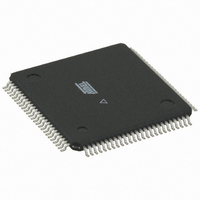
ATMEGA6490-16AI Atmel, ATMEGA6490-16AI Datasheet - Page 258

ATMEGA6490-16AI
Manufacturer Part Number
ATMEGA6490-16AI
Description
IC AVR MCU FLASH 64K 5V 100TQFP
Manufacturer
Atmel
Series
AVR® ATmegar
Datasheet
1.ATMEGA329-16AU.pdf
(392 pages)
Specifications of ATMEGA6490-16AI
Core Processor
AVR
Core Size
8-Bit
Speed
16MHz
Connectivity
SPI, UART/USART, USI
Peripherals
Brown-out Detect/Reset, LCD, POR, PWM, WDT
Number Of I /o
68
Program Memory Size
64KB (32K x 16)
Program Memory Type
FLASH
Eeprom Size
2K x 8
Ram Size
4K x 8
Voltage - Supply (vcc/vdd)
2.7 V ~ 5.5 V
Data Converters
A/D 8x10b
Oscillator Type
Internal
Operating Temperature
-40°C ~ 85°C
Package / Case
100-TQFP, 100-VQFP
For Use With
ATSTK600-TQFP100 - STK600 SOCKET/ADAPTER 100-TQFPATSTK504 - STARTER KIT AVR EXP MOD 100P LCD
Lead Free Status / RoHS Status
Contains lead / RoHS non-compliant
Available stocks
Company
Part Number
Manufacturer
Quantity
Price
Part Number:
ATMEGA6490-16AI
Manufacturer:
ATMEL/爱特梅尔
Quantity:
20 000
- Current page: 258 of 392
- Download datasheet (7Mb)
25.6.3
258
ATmega329/3290/649/6490
Scanning the Clock Pins
The AVR devices have many clock options selectable by fuses. These are: Internal RC Oscilla-
tor, External Clock, (High Frequency) Crystal Oscillator, Low-frequency Crystal Oscillator, and
Ceramic Resonator.
Figure 25-6
The Enable signal is supported with a general Boundary-scan cell, while the Oscillator/clock out-
put is attached to an observe-only cell. In addition to the main clock, the timer Oscillator is
scanned in the same way. The output from the internal RC Oscillator is not scanned, as this
Oscillator does not have external connections.
Figure 25-6. Boundary-scan Cells for Oscillators and Clock Options
Table 25-3
XTAL1/XTAL2 connections as well as 32kHz Timer Oscillator.
Table 25-3.
Notes:
Enable Signal
EXTCLKEN
OSCON
OSC32EN
From Digital Logic
1. Do not enable more than one clock source as main clock at a time.
2. Scanning an Oscillator output gives unpredictable results as there is a frequency drift between
3. The clock configuration is programmed by fuses. As a fuse is not changed run-time, the clock
the internal Oscillator and the JTAG TCK clock. If possible, scanning an external clock is
preferred.
configuration is considered fixed for a given application. The user is advised to scan the same
clock option as to be used in the final system. The enable signals are supported in the scan
chain because the system logic can disable clock options in sleep modes, thereby disconnect-
ing the Oscillator pins from the scan path if not provided.
summaries the scan registers for the external clock pin XTAL1, oscillators with
shows how each Oscillator with external connection is supported in the scan chain.
Scan Signals for the Oscillator
Previous
From
Cell
Scanned Clock Line
EXTCLK (XTAL1)
OSCCK
OSC32CK
ShiftDR
0
1
ClockDR
D
UpdateDR
Q
Next
Cell
To
D
G
Q
Clock Option
External Clock
External Crystal
External Ceramic Resonator
Low Freq. External Crystal
EXTEST
0
1
XTAL1/TOSC1
(1)(2)(3)
ENABLE
Oscillator
XTAL2/TOSC2
OUTPUT
Previous
From
Cell
ShiftDR
0
1
ClockDR
Scanned Clock
Line when not
D
FF1
Used
Q
0
1
1
Next
Cell
To
To System Logic
2552K–AVR–04/11
Related parts for ATMEGA6490-16AI
Image
Part Number
Description
Manufacturer
Datasheet
Request
R

Part Number:
Description:
Manufacturer:
Atmel Corporation
Datasheet:

Part Number:
Description:
IC AVR MCU FLASH 64K 64-QFN
Manufacturer:
Atmel
Datasheet:

Part Number:
Description:
IC AVR MCU FLASH 64K 64TQFP
Manufacturer:
Atmel
Datasheet:

Part Number:
Description:
IC AVR MCU FLASH 64K 5V 64TQFP
Manufacturer:
Atmel
Datasheet:

Part Number:
Description:
IC AVR MCU FLASH 64K 5V 64QFN
Manufacturer:
Atmel
Datasheet:

Part Number:
Description:
MCU AVR 64KB FLASH 16MHZ 64QFN
Manufacturer:
Atmel
Datasheet:

Part Number:
Description:
IC MCU AVR FLASH 64K 64TQFP
Manufacturer:
Atmel
Datasheet:

Part Number:
Description:
Manufacturer:
Atmel Corporation
Datasheet:

Part Number:
Description:
Manufacturer:
ATMEL Corporation
Datasheet:

Part Number:
Description:
Manufacturer:
ATMEL Corporation
Datasheet:

Part Number:
Description:
IC AVR MCU 64K 16MHZ 5V 64TQFP
Manufacturer:
Atmel
Datasheet:

Part Number:
Description:
IC AVR MCU 64K 16MHZ 5V 64-QFN
Manufacturer:
Atmel
Datasheet:

Part Number:
Description:
IC AVR MCU 64K 16MHZ COM 64-TQFP
Manufacturer:
Atmel
Datasheet:

Part Number:
Description:
IC AVR MCU 64K 16MHZ IND 64-TQFP
Manufacturer:
Atmel
Datasheet:

Part Number:
Description:
IC AVR MCU 64K 16MHZ COM 64-QFN
Manufacturer:
Atmel
Datasheet:


