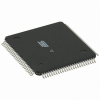
ATMEGA6490-16AI Atmel, ATMEGA6490-16AI Datasheet - Page 38

ATMEGA6490-16AI
Manufacturer Part Number
ATMEGA6490-16AI
Description
IC AVR MCU FLASH 64K 5V 100TQFP
Manufacturer
Atmel
Series
AVR® ATmegar
Datasheet
1.ATMEGA329-16AU.pdf
(392 pages)
Specifications of ATMEGA6490-16AI
Core Processor
AVR
Core Size
8-Bit
Speed
16MHz
Connectivity
SPI, UART/USART, USI
Peripherals
Brown-out Detect/Reset, LCD, POR, PWM, WDT
Number Of I /o
68
Program Memory Size
64KB (32K x 16)
Program Memory Type
FLASH
Eeprom Size
2K x 8
Ram Size
4K x 8
Voltage - Supply (vcc/vdd)
2.7 V ~ 5.5 V
Data Converters
A/D 8x10b
Oscillator Type
Internal
Operating Temperature
-40°C ~ 85°C
Package / Case
100-TQFP, 100-VQFP
For Use With
ATSTK600-TQFP100 - STK600 SOCKET/ADAPTER 100-TQFPATSTK504 - STARTER KIT AVR EXP MOD 100P LCD
Lead Free Status / RoHS Status
Contains lead / RoHS non-compliant
Available stocks
Company
Part Number
Manufacturer
Quantity
Price
Part Number:
ATMEGA6490-16AI
Manufacturer:
ATMEL/爱特梅尔
Quantity:
20 000
- Current page: 38 of 392
- Download datasheet (7Mb)
9.7.3
9.7.4
9.7.5
9.7.6
9.7.7
38
ATmega329/3290/649/6490
Brown-out Detector
Internal Voltage Reference
Watchdog Timer
Port Pins
JTAG Interface and On-chip Debug System
the Analog Comparator is automatically disabled. However, if the Analog Comparator is set up
to use the Internal Voltage Reference as input, the Analog Comparator should be disabled in all
sleep modes. Otherwise, the Internal Voltage Reference will be enabled, independent of sleep
mode. Refer to
Comparator.
If the Brown-out Detector is not needed by the application, this module should be turned off. If
the Brown-out Detector is enabled by the BODLEVEL Fuses, it will be enabled in all sleep
modes, and hence, always consume power. In the deeper sleep modes, this will contribute sig-
nificantly to the total current consumption. Refer to
on how to configure the Brown-out Detector.
The Internal Voltage Reference will be enabled when needed by the Brown-out Detection, the
Analog Comparator or the ADC. If these modules are disabled as described in the sections
above, the internal voltage reference will be disabled and it will not be consuming power. When
turned on again, the user must allow the reference to start up before the output is used. If the
reference is kept on in sleep mode, the output can be used immediately. Refer to
age Reference” on page 44
If the Watchdog Timer is not needed in the application, the module should be turned off. If the
Watchdog Timer is enabled, it will be enabled in all sleep modes, and hence, always consume
power. In the deeper sleep modes, this will contribute significantly to the total current consump-
tion. Refer to
When entering a sleep mode, all port pins should be configured to use minimum power. The
most important is then to ensure that no pins drive resistive loads. In sleep modes where both
the I/O clock (clk
be disabled. This ensures that no power is consumed by the input logic when not needed. In
some cases, the input logic is needed for detecting wake-up conditions, and it will then be
enabled. Refer to the section
which pins are enabled. If the input buffer is enabled and the input signal is left floating or have
an analog signal level close to V
For analog input pins, the digital input buffer should be disabled at all times. An analog signal
level close to V
input buffers can be disabled by writing to the Digital Input Disable Registers (DIDR1 and
DIDR0). Refer to
Input Disable Register 0” on page 227
If the On-chip debug system is enabled by the OCDEN Fuse and the chip enter Power down or
Power save sleep mode, the main clock source remains enabled. In these sleep modes, this will
contribute significantly to the total current consumption. There are three alternative ways to
avoid this:
•
•
Disable OCDEN Fuse.
Disable JTAGEN Fuse.
“Watchdog Timer” on page 45
CC
“Analog Comparator” on page 207
I/O
“DIDR1 – Digital Input Disable Register 1” on page 210
/2 on an input pin can cause significant current even in active mode. Digital
) and the ADC clock (clk
for details on the start-up time.
“Digital Input Enable and Sleep Modes” on page 64
CC
/2, the input buffer will use excessive power.
for details.
ADC
for details on how to configure the Watchdog Timer.
) are stopped, the input buffers of the device will
“Brown-out Detection” on page 43
for details on how to configure the Analog
and
“DIDR0 – Digital
2552K–AVR–04/11
“Internal Volt-
for details on
for details
Related parts for ATMEGA6490-16AI
Image
Part Number
Description
Manufacturer
Datasheet
Request
R

Part Number:
Description:
Manufacturer:
Atmel Corporation
Datasheet:

Part Number:
Description:
IC AVR MCU FLASH 64K 64-QFN
Manufacturer:
Atmel
Datasheet:

Part Number:
Description:
IC AVR MCU FLASH 64K 64TQFP
Manufacturer:
Atmel
Datasheet:

Part Number:
Description:
IC AVR MCU FLASH 64K 5V 64TQFP
Manufacturer:
Atmel
Datasheet:

Part Number:
Description:
IC AVR MCU FLASH 64K 5V 64QFN
Manufacturer:
Atmel
Datasheet:

Part Number:
Description:
MCU AVR 64KB FLASH 16MHZ 64QFN
Manufacturer:
Atmel
Datasheet:

Part Number:
Description:
IC MCU AVR FLASH 64K 64TQFP
Manufacturer:
Atmel
Datasheet:

Part Number:
Description:
Manufacturer:
Atmel Corporation
Datasheet:

Part Number:
Description:
Manufacturer:
ATMEL Corporation
Datasheet:

Part Number:
Description:
Manufacturer:
ATMEL Corporation
Datasheet:

Part Number:
Description:
IC AVR MCU 64K 16MHZ 5V 64TQFP
Manufacturer:
Atmel
Datasheet:

Part Number:
Description:
IC AVR MCU 64K 16MHZ 5V 64-QFN
Manufacturer:
Atmel
Datasheet:

Part Number:
Description:
IC AVR MCU 64K 16MHZ COM 64-TQFP
Manufacturer:
Atmel
Datasheet:

Part Number:
Description:
IC AVR MCU 64K 16MHZ IND 64-TQFP
Manufacturer:
Atmel
Datasheet:

Part Number:
Description:
IC AVR MCU 64K 16MHZ COM 64-QFN
Manufacturer:
Atmel
Datasheet:


