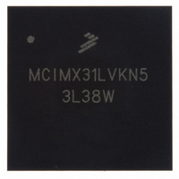
MCIMX31LVKN5 Freescale Semiconductor, MCIMX31LVKN5 Datasheet - Page 21

MCIMX31LVKN5
Manufacturer Part Number
MCIMX31LVKN5
Description
IC MPU MAP I.MX31L 457-MAPBGA
Manufacturer
Freescale Semiconductor
Series
i.MX31r
Datasheet
1.MCIMX31LITEKITC.pdf
(122 pages)
Specifications of MCIMX31LVKN5
Core Processor
ARM11
Core Size
32-Bit
Speed
532MHz
Connectivity
1-Wire, ATA, EBI/EMI, FIR, I²C, MMC/SD, PCMCIA, SIM, SPI, SSI, UART/USART, USB, USB OTG
Peripherals
DMA, LCD, POR, PWM, WDT
Program Memory Type
ROMless
Ram Size
16K x 8
Voltage - Supply (vcc/vdd)
1.22 V ~ 3.3 V
Oscillator Type
External
Operating Temperature
0°C ~ 70°C
Package / Case
457-MAPBGA
Lead Free Status / RoHS Status
Lead free / RoHS Compliant
Number Of I /o
-
Eeprom Size
-
Program Memory Size
-
Data Converters
-
Available stocks
Company
Part Number
Manufacturer
Quantity
Price
Company:
Part Number:
MCIMX31LVKN5
Manufacturer:
ADI
Quantity:
9 710
Company:
Part Number:
MCIMX31LVKN5
Manufacturer:
Freescale Semiconductor
Quantity:
10 000
Company:
Part Number:
MCIMX31LVKN5B
Manufacturer:
Freescale Semiconductor
Quantity:
10 000
Company:
Part Number:
MCIMX31LVKN5BR2
Manufacturer:
Freescale Semiconductor
Quantity:
10 000
Company:
Part Number:
MCIMX31LVKN5C
Manufacturer:
FREESCALE
Quantity:
1 831
Company:
Part Number:
MCIMX31LVKN5C
Manufacturer:
FREESCALE
Quantity:
748
Company:
Part Number:
MCIMX31LVKN5C
Manufacturer:
Freescale Semiconductor
Quantity:
10 000
Part Number:
MCIMX31LVKN5C
Manufacturer:
FREESCALE
Quantity:
20 000
Company:
Part Number:
MCIMX31LVKN5R2
Manufacturer:
IBM
Quantity:
284
Part Number:
MCIMX31LVKN5R2
Manufacturer:
FREESCALE
Quantity:
20 000
Freescale Semiconductor
NVCC2, NVCC21, NVCC22
IOQVDD, NVCC1, NVCC3–10, NVCC2, NVCC21, NVCC22
IOQVDD, NVCC1, NVCC3–10
FVCC, MVCC, SVCC, UVCC
QVCC, QVCC1, QVCC4
QVCC, QVCC1, QVCC4
Figure 3. Option 1 Power-Up Sequence (Silicon Revision 2.0)
Hold POR Asserted
Figure 4. Option 2 Power-Up Sequence (Silicon Revision 2.0)
Hold POR Asserted
Release POR
Release POR
1, 3, 5
4
4
MCIMX31/MCIMX31L Technical Data, Rev. 4.1
FVCC, MVCC, SVCC, UVCC
1
1
1
1, 2
1, 2,3
1,3
Notes:
1
2
3
4
Notes:
1
2
3
4
5
The board design must guarantee that supplies reach
90% level before transition to the next state, using Power
Management IC or other means.
The NVCC1 supply must not precede IOQVDD by more
than 0.2 V until IOQVDD has reached 1.5 V. If IOQVDD
is powered up first, there are no restrictions.
Raising NVCC2, NVCC21, and NVCC22 at the same
time as IOQVDD does not produce the slight increase in
current drain on IOQVDD (as described in
Note 5).
Unlike the power-up sequence for Silicon Revision 1.2,
FUSE_VDD should not be driven on power-up for Silicon
Revision 2.0. This supply is dedicated for fuse burning
(programming), and should not be driven upon boot-up.
The board design must guarantee that supplies reach
90% level before transition to the next state, using Power
Management IC or other means.
The NVCC1 supply must not precede IOQVDD by more
than 0.2 V until IOQVDD has reached 1.5 V. If IOQVDD
is powered up first, there are no restrictions.
The parallel paths in the flow indicate that supply group
NVCC2, NVCC21, and NVCC22, and supply group
FVCC, MVCC, SVCC, and UVCC ramp-ups are
independent. Note that this power-up sequence is
backward compatible to Silicon Revs. 1.15 and 1.2,
because NVCC2x ramp-up proceeding PLL supplies is
allowed.
Unlike the power-up sequence for Silicon Revision 1.2,
FUSE_VDD should not be driven on power-up for Silicon
Revision 2.0. This supply is dedicated for fuse burning
(programming), and should not be driven upon boot-up.
Raising IOQVDD before NVCC21 produces a slight
increase in current drain on IOQVDD of approximately
3–5 mA. The current increase will not damage the IC.
Refer to Errata ID TLSbo91750 for details.
Electrical Characteristics
Figure
3,
21


