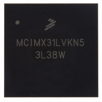
MCIMX31LVKN5 Freescale Semiconductor, MCIMX31LVKN5 Datasheet - Page 38

MCIMX31LVKN5
Manufacturer Part Number
MCIMX31LVKN5
Description
IC MPU MAP I.MX31L 457-MAPBGA
Manufacturer
Freescale Semiconductor
Series
i.MX31r
Datasheet
1.MCIMX31LITEKITC.pdf
(122 pages)
Specifications of MCIMX31LVKN5
Core Processor
ARM11
Core Size
32-Bit
Speed
532MHz
Connectivity
1-Wire, ATA, EBI/EMI, FIR, I²C, MMC/SD, PCMCIA, SIM, SPI, SSI, UART/USART, USB, USB OTG
Peripherals
DMA, LCD, POR, PWM, WDT
Program Memory Type
ROMless
Ram Size
16K x 8
Voltage - Supply (vcc/vdd)
1.22 V ~ 3.3 V
Oscillator Type
External
Operating Temperature
0°C ~ 70°C
Package / Case
457-MAPBGA
Lead Free Status / RoHS Status
Lead free / RoHS Compliant
Number Of I /o
-
Eeprom Size
-
Program Memory Size
-
Data Converters
-
Available stocks
Company
Part Number
Manufacturer
Quantity
Price
Company:
Part Number:
MCIMX31LVKN5
Manufacturer:
ADI
Quantity:
9 710
Company:
Part Number:
MCIMX31LVKN5
Manufacturer:
Freescale Semiconductor
Quantity:
10 000
Company:
Part Number:
MCIMX31LVKN5B
Manufacturer:
Freescale Semiconductor
Quantity:
10 000
Company:
Part Number:
MCIMX31LVKN5BR2
Manufacturer:
Freescale Semiconductor
Quantity:
10 000
Company:
Part Number:
MCIMX31LVKN5C
Manufacturer:
FREESCALE
Quantity:
1 831
Company:
Part Number:
MCIMX31LVKN5C
Manufacturer:
FREESCALE
Quantity:
748
Company:
Part Number:
MCIMX31LVKN5C
Manufacturer:
Freescale Semiconductor
Quantity:
10 000
Part Number:
MCIMX31LVKN5C
Manufacturer:
FREESCALE
Quantity:
20 000
Company:
Part Number:
MCIMX31LVKN5R2
Manufacturer:
IBM
Quantity:
284
Part Number:
MCIMX31LVKN5R2
Manufacturer:
FREESCALE
Quantity:
20 000
Electrical Characteristics
1
2
4.3.9
This section provides electrical parametrics and timings for EMI module.
4.3.9.1
The NFC supports normal timing mode, using two flash clock cycles for one access of RE and WE. AC
timings are provided as multiplications of the clock cycle and fixed delay.
and
for normal mode, and
38
Phase lock time
Maximum allowed PLL supply voltage ripple
Maximum allowed PLL supply voltage ripple
Maximum allowed PLL supply voltage ripple
PLL output clock phase jitter
PLL output clock period jitter
The user or board designer must take into account that the use of a frequency other than 26 MHz would require adjustment to
the DPTC–DVFS table, which is incorporated into operating system code.
The PLL reference frequency must be ≤ 35 MHz. Therefore, for frequencies between 35 MHz and 70 MHz, program the
predivider to divide by 2 or more. If the CKIH frequency is above 70 MHz, program the predivider to 3 or more. For PD bit
description, see the reference manual.
Figure 26
EMI Electrical Specifications
NAND Flash Controller Interface (NFC)
depict the relative timing requirements among different signals of the NFC at module level,
NFCE
NFWE
NFIO[7:0]
NFCLE
NFALE
Parameter
Table 32
Figure 23. Command Latch Cycle Timing DIagram
lists the timing parameters.
Table 31. DPLL Specifications (continued)
MCIMX31/MCIMX31L Technical Data, Rev. 4.1
NF6
NF3
NF1
Min
—
—
—
—
—
—
Command
NF8
NF5
Typ
—
—
—
—
—
—
NF9
NF7
Max
100
420
5.2
NF2
25
20
25
NF4
Unit
mV 50 kHz < F
mV F
mV F
ns
ps
µs
Figure
In addition to the frequency
Measured on CLKO pin
Measured on CLKO pin
modulation
modulation
23,
< 50 kHz
> 300 kHz
Figure
modulation
Freescale Semiconductor
Comments
24,
< 300 kHz
Figure
25,


