MCIMX31LVKN5 Freescale Semiconductor, MCIMX31LVKN5 Datasheet - Page 43
MCIMX31LVKN5
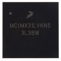
Manufacturer Part Number
MCIMX31LVKN5
Description
IC MPU MAP I.MX31L 457-MAPBGA
Manufacturer
Freescale Semiconductor
Series
i.MX31r
Datasheet
1.MCIMX31LITEKITC.pdf
(122 pages)
Specifications of MCIMX31LVKN5
Core Processor
ARM11
Core Size
32-Bit
Speed
532MHz
Connectivity
1-Wire, ATA, EBI/EMI, FIR, I²C, MMC/SD, PCMCIA, SIM, SPI, SSI, UART/USART, USB, USB OTG
Peripherals
DMA, LCD, POR, PWM, WDT
Program Memory Type
ROMless
Ram Size
16K x 8
Voltage - Supply (vcc/vdd)
1.22 V ~ 3.3 V
Oscillator Type
External
Operating Temperature
0°C ~ 70°C
Package / Case
457-MAPBGA
Lead Free Status / RoHS Status
Lead free / RoHS Compliant
Number Of I /o
-
Eeprom Size
-
Program Memory Size
-
Data Converters
-
Available stocks
Company
Part Number
Manufacturer
Quantity
Price
Company:

Part Number:
MCIMX31LVKN5
Manufacturer:
ADI
Quantity:
9 710
Company:
Part Number:
MCIMX31LVKN5
Manufacturer:
Freescale Semiconductor
Quantity:
10 000
Company:
Part Number:
MCIMX31LVKN5B
Manufacturer:
Freescale Semiconductor
Quantity:
10 000
Company:
Part Number:
MCIMX31LVKN5BR2
Manufacturer:
Freescale Semiconductor
Quantity:
10 000
Company:
Part Number:
MCIMX31LVKN5C
Manufacturer:
FREESCALE
Quantity:
1 831
Company:
Part Number:
MCIMX31LVKN5C
Manufacturer:
FREESCALE
Quantity:
748
Company:
Part Number:
MCIMX31LVKN5C
Manufacturer:
Freescale Semiconductor
Quantity:
10 000
Part Number:
MCIMX31LVKN5C
Manufacturer:
FREESCALE
Quantity:
20 000
Company:
Part Number:
MCIMX31LVKN5R2
Manufacturer:
IBM
Quantity:
284
Part Number:
MCIMX31LVKN5R2
Manufacturer:
FREESCALE
Quantity:
20 000


Figure
basic WEIM accesses to external memory devices with the timing parameters mentioned in
Table 33
Freescale Semiconductor
28,
1
2
3
WE10
WE11
WE18
WE19
WE20
WE22
WE23
WE12
WE13
WE14
WE15
WE16
WE17
WE21
for specific control parameter settings.
WE8
WE9
Applies to rising edge timing
BCLK parameters are being measured from the 50% VDD.
The actual cycle time is derived from the AHB bus clock frequency.
ID
Figure
High is defined as 80% of signal value and low is defined as 20% of signal
value.
Test conditions: load capacitance, 25 pF. Recommended drive strength for all
controls, address, and BCLK is Max drive.
Clock rise to Output Data Invalid
Clock rise to Input Data Invalid, FCE=0
Clock rise/fall to OE Invalid
Clock rise/fall to EB[x] Valid
Clock rise/fall to EB[x] Invalid
Clock rise/fall to LBA Valid
Clock rise/fall to LBA Invalid
Clock rise/fall to Output Data Valid
Input Data Valid to Clock rise, FCE=0
ECB setup time, FCE=0
ECB hold time, FCE=0
DTACK setup time
DTACK hold time
BCLK High Level Width
BCLK Low Level Width
BCLK Cycle time
29,
Figure
Table 33. WEIM Bus Timing Parameters (continued)
30,
FCE=1
FCE=1
1
2
1
Figure
MCIMX31/MCIMX31L Technical Data, Rev. 4.1
2, 3
2, 3
Parameter
31,
FCE=1
FCE=1
Figure
NOTE
32, and
Figure 33
depict some examples of
–2.5
–2.5
Min
2.5
6.5
3.5
4.5
–3
–3
–3
–3
–3
–2
–2
–2
—
—
15
8
2
0
T/2 – 3
T/2 – 3
Electrical Characteristics
Max
—
—
—
—
—
—
—
3
3
3
3
3
4
4
Unit
ns
ns
ns
ns
ns
ns
ns
ns
ns
ns
ns
ns
ns
ns
ns
ns
43
Related parts for MCIMX31LVKN5
Image
Part Number
Description
Manufacturer
Datasheet
Request
R

Part Number:
Description:
Multimedia Applications Processors
Manufacturer:
FREESCALE [Freescale Semiconductor, Inc]
Datasheet:

Part Number:
Description:
MCIMX-LVDS1
Manufacturer:
Freescale Semiconductor
Datasheet:

Part Number:
Description:
Manufacturer:
Freescale Semiconductor, Inc
Datasheet:
Part Number:
Description:
Manufacturer:
Freescale Semiconductor, Inc
Datasheet:
Part Number:
Description:
Manufacturer:
Freescale Semiconductor, Inc
Datasheet:
Part Number:
Description:
Manufacturer:
Freescale Semiconductor, Inc
Datasheet:
Part Number:
Description:
Manufacturer:
Freescale Semiconductor, Inc
Datasheet:
Part Number:
Description:
Manufacturer:
Freescale Semiconductor, Inc
Datasheet:
Part Number:
Description:
Manufacturer:
Freescale Semiconductor, Inc
Datasheet:
Part Number:
Description:
Manufacturer:
Freescale Semiconductor, Inc
Datasheet:
Part Number:
Description:
Manufacturer:
Freescale Semiconductor, Inc
Datasheet:
Part Number:
Description:
Manufacturer:
Freescale Semiconductor, Inc
Datasheet:
Part Number:
Description:
Manufacturer:
Freescale Semiconductor, Inc
Datasheet:
Part Number:
Description:
Manufacturer:
Freescale Semiconductor, Inc
Datasheet:
Part Number:
Description:
Manufacturer:
Freescale Semiconductor, Inc
Datasheet: