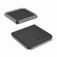
HSP50210JI-52Z Intersil, HSP50210JI-52Z Datasheet - Page 34

HSP50210JI-52Z
Manufacturer Part Number
HSP50210JI-52Z
Description
IC DEMODULATOR COSTAS 84-PLCC
Manufacturer
Intersil
Datasheet
1.HSP50210JC-52Z.pdf
(51 pages)
Specifications of HSP50210JI-52Z
Function
Demodulator
Frequency
52MHz
Rf Type
AM, FM
Package / Case
84-PLCC
Lead Free Status / RoHS Status
Lead free / RoHS Compliant
Available stocks
Company
Part Number
Manufacturer
Quantity
Price
Part Number:
HSP50210JI-52Z
Manufacturer:
INTERSIL
Quantity:
20 000
POSITION
POSITION
POSITION
POSITION
31-8
31-8
31-8
BIT
BIT
BIT
BIT
5-2
1-0
7-3
2-0
7-3
2-0
7
6
Phase Offset
Shift Factor
Not Used
Reserved
Discriminator Delay
Not Used
Frequency Offset
Shift Factor
Not Used
Reserved
Lead/Lag to Serial
Output Routing
FUNCTION
FUNCTION
FUNCTION
FUNCTION
TABLE 18. CARRIER PHASE ERROR DETECTOR CONTROL REGISTER (Continued)
34
TABLE 20. FREQUENCY ERROR DETECTOR CONTROL REGISTER
TABLE 21. CARRIER LOOP FILTER CONTROL REGISTER #1
TABLE 19. FREQUENCY DETECTOR CONTROL REGISTER
These bits set the phase offset added (modulo 2
Converter. The phase offset is represented as a 4-bit fractional 2’s Complement value with the following
binary format:
Phase Offset = -2
This format provides a range from 0.875 to -1 (0111 to 1000) which corresponds to phase offset settings
from 7
The bits set the left shift required by the Carrier Phase Error Detector. These two bits specify a left shift
of 0, 1, 2 or 3 places. MSBs are discarded and LSBs are zero-filled. Bit 1 is the MSB.
No programming required.
Reserved. Set to 0 for proper operation.
The frequency detector (discriminator) computes frequency by subtracting a delayed phase term from
the current phase term (d
set the delay as given by:
Delay = 2
where K is the 3-bit value programmed here. Delays of 1, 2, 4, 8, and 16 are possible.
No programming required.
These bits set the frequency offset added (modulo) to the frequency output of the discriminator. The frequency
offset is represented as a 5-bit fractional 2’s complement value with the following binary format:
Frequency Offset = -2
This format provides a range from 0.9375 to -1.0 (0111 to 1000). The range and resolution of the
frequency offset depend on the discriminator delay and input rate. The frequency offset is added to the
5 MSBs of the discriminator output. Note: Set the frequency offset to 0 when using frequency aided
acquisition with PSK waveforms.
These bits set the left shift required by the Frequency Error Detector. These two bits set a left shift of 0,
1, 2, 3, or 4 places. Bit 2 is the MSB. Values greater than 4 are invalid. Note: Set the shift factor to 0 when
using frequency aided acquisition with PSK waveforms.
No programming required.
Reserved. Set to 0 for proper operation.
0 = The Carrier Loop Filter’s Lag Accumulator is routed to the Serial Output Controller.
1 = The lead and lag paths in the Carrier Loop Filter are summed and routed to the Serial Output
Controller.
π
/8 to -
K
,
π
respectively. Resolution of 22.5° is provided. Bit position 5 is the MSB.
DESTINATION ADDRESS = 3
DESTINATION ADDRESS = 4
DESTINATION ADDRESS = 5
DESTINATION ADDRESS = 6
0
. 2
-1
0
HSP50210
2
. 2
-2
θ
-1
2
/dt). A programmable delay is used to set the discriminator gain. These bits
-3.
2
-2
2
-3
2
-4.
DESCRIPTION
DESCRIPTION
DESCRIPTION
DESCRIPTION
π
) to the phase output of the Cartesian-to-Polar
July 2, 2008
FN3652.5


