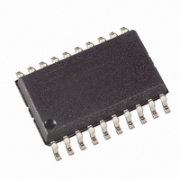
U3741BM-P2FL Atmel, U3741BM-P2FL Datasheet - Page 11

U3741BM-P2FL
Manufacturer Part Number
U3741BM-P2FL
Description
IC RECEIVER PLL 300KHZ 20-SOIC
Manufacturer
Atmel
Datasheet
1.U3741BM-P3FLG3.pdf
(32 pages)
Specifications of U3741BM-P2FL
Frequency
300MHz ~ 450MHz
Sensitivity
-109dBm
Data Rate - Maximum
10 kBaud
Modulation Or Protocol
ASK, FSK
Applications
RKE, Remote Control Systems
Current - Receiving
8.2mA
Data Interface
PCB, Surface Mount
Antenna Connector
PCB, Surface Mount
Voltage - Supply
4.5 V ~ 5.5 V
Operating Temperature
-40°C ~ 105°C
Package / Case
20-SOIC (0.300", 7.50mm Width)
Lead Free Status / RoHS Status
Contains lead / RoHS non-compliant
Features
-
Memory Size
-
Polling Mode
Sleep Mode
4662B–RKE–10/04
•
•
•
The clock cycle of some function blocks depends on the selected baud rate range
(BR_Range) which is defined in the OPMODE register. This clock cycle T
by the following formulas for further reference:
According to Figure 3 on page 6, the receiver stays in polling mode in a continuous
cycle of three different modes. In sleep mode, the signal processing circuitry is disabled
for the time period T
period, T
check mode, the incoming data stream is analyzed bit by bit against a valid transmitter
signal. If no valid signal is present, the receiver is set back to sleep mode after the
period T
age value for T
and T
polling mode is dependent on the duty cycle of the active mode and can be calculated
as:
During T
tee the reception of a transmitted command, the transmitter must start the telegram with
an adequate preburst. The required length of the preburst is dependent on the polling
parameters T
(T
be tested.
The following formula indicates how to calculate the preburst length.
T
The length of period T
the extension factor X
T
In US and European applications, the maximum value of T
set to 1. The time resolution is about 2 ms in that case. The sleep time can be extended
to almost half a second by setting X
bit X
I
T
Spoll
BR_Range =
Preburst
Clk
Sleep
Start,µC
. It is calculated to be:
USA Applications
(f
Europe Applications
(f
Other applications
(T
characteristic is given as a function of T
SleepTemp
XTO
XTO
=
Bitcheck
Clk
=
I
------------------------------------------------------------------------------------------------------------
). T
Soff
Bitcheck
Sleep
Sleep
is dependent on f
Startup
= 4.90625 MHz, MODE = L, T
= 6.76438 MHz, MODE = H, T
T
Sleep
Bitcheck
the current consumption is I
resulting in a different mode of action as described below:
and T
T
Sleep
, all signal processing circuits are enabled and settled. In the following bit
. This period varies check by check as it is a statistical process. An aver-
T
Sleep
Bitcheck
Sleep
+ T
X
BR_Range0:
BR_Range1:
BR_Range2:
BR_Range3:
, T
thus depends on the actual bit rate and the number of bits (N
Sleep
Startup
Startup
+
+
Sleep
Startup
I
Son
T
Sleep
is given in “Electrical Characteristics” on page 23. During T
Sleep
Startup
, the receiver is not sensitive to a transmitter signal. To guaran-
1024
+ T
while consuming a low current of I
, T
, according to Figure 10 on page 13, and the basic clock cycle
XTO
is defined by the 5-bit word Sleep of the OPMODE register,
T
Bitcheck
Bitcheck
+
Startup
and on the logical state of pin MODE. The electrical
T
T
Bitcheck
Clk
T
T
T
T
+
+ T
XClk
XClk
XClk
XClk
and the startup time of a connected microcontroller
Sleep
T
Bitcheck
Start_ C
Clk
= 8
= 4
= 2
= 1
Clk
to 8. X
S
= 2.0383 µs)
= 2.0697 µs)
= I
Clk
T
T
T
T
).
Son
Clk
Clk
Clk
Clk
Sleep
. The average current consumption in
can be set to 8 by bit X
Sleep
S
= I
is about 60 ms if X
Soff
. During the start-up
U3741BM
XClk
SleepStd
is defined
Bitcheck
Sleep
Startup
or by
) to
11
is


