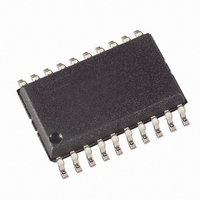
U3741BM-P2FL Atmel, U3741BM-P2FL Datasheet - Page 12

U3741BM-P2FL
Manufacturer Part Number
U3741BM-P2FL
Description
IC RECEIVER PLL 300KHZ 20-SOIC
Manufacturer
Atmel
Datasheet
1.U3741BM-P3FLG3.pdf
(32 pages)
Specifications of U3741BM-P2FL
Frequency
300MHz ~ 450MHz
Sensitivity
-109dBm
Data Rate - Maximum
10 kBaud
Modulation Or Protocol
ASK, FSK
Applications
RKE, Remote Control Systems
Current - Receiving
8.2mA
Data Interface
PCB, Surface Mount
Antenna Connector
PCB, Surface Mount
Voltage - Supply
4.5 V ~ 5.5 V
Operating Temperature
-40°C ~ 105°C
Package / Case
20-SOIC (0.300", 7.50mm Width)
Lead Free Status / RoHS Status
Contains lead / RoHS non-compliant
Features
-
Memory Size
-
Figure 8. Polling Mode Flow Chart
12
U3741BM
NO
Sleep Mode:
All circuits for signal processing are
disabled. Only XTO and polling logic is
enabled.
Output level on pin IC_ACTIVE => low
I
T
Start-up Mode:
The signal processing circuits are
enabled. After the start-up time (T
circuits are in stable condition and ready
to receive.
I
T
Bit-check Mode:
The incomming data stream is analyzed.
If the timing indicates a valid transmitter
signal, the receiver is set to receiving
mode. Otherwise it is set to Sleep mode.
I
T
Receiving Mode:
The receiver is turned on permanently
and passes the data stream to the
connected microcontroller. It can be set to
Sleep mode through an OFF command
via pin DATA or ENABLE
I
S
S
S
S
Sleep
Startup
Bit-check
= I
= I
= I
= I
SON
SON
Son
SON
= Sleep
OFF command
X
X
as long as every bit check is OK. If the bit check fails once, this bit is set back to 0 auto-
matically resulting in a regular sleep time. This functionality can be used to save current
in presence of a modulated disturber similar to an expected transmitter signal. The con-
nected microcontroller is rarely activated in that condition. If the disturber disappears,
the receiver switches back to regular polling and is again sensitive to appropriate trans-
mitter signals.
According to Table 7 on page 19, the highest register value of Sleep sets the receiver to
a permanent sleep condition. The receiver remains in that condition until another value
for Sleep is programmed into the OPMODE register. This function is desirable where
several devices share a single data line.
Bit-check
X
SleepStd
SleepTemp
OK?
Sleep
YES
1024
= 1 implies the standard extension factor. The sleep time is always extended.
= 1 implies the temporary extension factor. The extended sleep time is used
T
Clk
Startup
) all
Sleep:
X
T
T
T
Clk
Startup
Bit-check
Sleep
:
:
:
:
5-bit word defined by Sleep0 to Sleep4 in
OPMODE register
Extension factor defined by X
according to Table 8
Basic clock cycle defined by f
MODE
Is defined by the selected baud rate range
and T
by Baud0 and Baud1 in the OPMODE
register.
Depends on the result of the bit check.
If the bit check is ok, T
on the number of bits to be checked
(N
If the bit check fails, the average time
period for that check depends on the
selected baud-rate range on T
baud-rate range is defined by Baud0 and
Baud1 in the OPMODE register.
Bit-checked
Clk
. The baud-rate range is defined
) and on the utilized data rate.
Bit-check
depends
SleepTemp
XTO
Clk
. The
and pin
4662B–RKE–10/04


