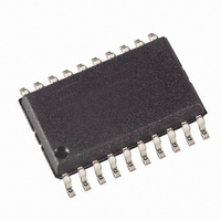
U3741BM-P2FL Atmel, U3741BM-P2FL Datasheet - Page 16

U3741BM-P2FL
Manufacturer Part Number
U3741BM-P2FL
Description
IC RECEIVER PLL 300KHZ 20-SOIC
Manufacturer
Atmel
Datasheet
1.U3741BM-P3FLG3.pdf
(32 pages)
Specifications of U3741BM-P2FL
Frequency
300MHz ~ 450MHz
Sensitivity
-109dBm
Data Rate - Maximum
10 kBaud
Modulation Or Protocol
ASK, FSK
Applications
RKE, Remote Control Systems
Current - Receiving
8.2mA
Data Interface
PCB, Surface Mount
Antenna Connector
PCB, Surface Mount
Voltage - Supply
4.5 V ~ 5.5 V
Operating Temperature
-40°C ~ 105°C
Package / Case
20-SOIC (0.300", 7.50mm Width)
Lead Free Status / RoHS Status
Contains lead / RoHS non-compliant
Features
-
Memory Size
-
Figure 14. Synchronization of the Demodulator Output
Figure 15. Debouncing of the Demodulator Output
Figure 16. Steady L State Limited DATA Output Pattern after Transmission
Switching the Receiver Back
to Sleep Mode
16
counter
Dem_out
DATA
Clock Bitcheck
Dem_out
DATA
U3741BM
Enable IC
Bit check
Dem_out
DATA
Sleep mode
Lim_min
T
XClk
t
ee
CV_Lim < Lim_max
After the end of a data transmission, the receiver remains active and random noise
pulses appear at pin DATA. The edge-to-edge time period t
noise pulses is equal to or slightly higher than T
The receiver can be set back to polling mode via pin DATA or via pin ENABLE.
When using pin DATA, this pin must be pulled to low for the period t1 by the connected
microcontroller. Figure 17 illustrates the timing of the OFF command (see also Figure 21
on page 21). The minimum value of t1 depends on the BR_Range. The maximum value
for t1 is not limited but it is recommended not to exceed the specified value to prevent
erasing the reset marker. This item is explained in more detail in the section “Configura-
tion of the Receiver” on page 17. Setting the receiver to sleep mode via DATA is
achieved by programming bit 1 of the OPMODE register to 1. Only one sync pulse (t3) is
issued.
The duration of the OFF command is determined by the sum of t1, t2 and t10. After the
OFF command, the sleep time T
is limited. The resulting time constant
tor may not be exceeded to ensure proper operation.
Bit check mode
t
ee
tmin1
CV_Lim < Lim_min or CV_Lim
Receiving mode
t
ee
Sleep
elapses. Note that the capacitive load at pin DATA
Lim_max
together with an optional external pull-up resis-
tmin2
DATA_min
tmin2
t
DATA_L_max
.
ee
of the majority of these
4662B–RKE–10/04


