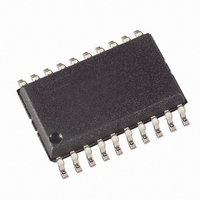
U3741BM-P2FL Atmel, U3741BM-P2FL Datasheet - Page 14

U3741BM-P2FL
Manufacturer Part Number
U3741BM-P2FL
Description
IC RECEIVER PLL 300KHZ 20-SOIC
Manufacturer
Atmel
Datasheet
1.U3741BM-P3FLG3.pdf
(32 pages)
Specifications of U3741BM-P2FL
Frequency
300MHz ~ 450MHz
Sensitivity
-109dBm
Data Rate - Maximum
10 kBaud
Modulation Or Protocol
ASK, FSK
Applications
RKE, Remote Control Systems
Current - Receiving
8.2mA
Data Interface
PCB, Surface Mount
Antenna Connector
PCB, Surface Mount
Voltage - Supply
4.5 V ~ 5.5 V
Operating Temperature
-40°C ~ 105°C
Package / Case
20-SOIC (0.300", 7.50mm Width)
Lead Free Status / RoHS Status
Contains lead / RoHS non-compliant
Features
-
Memory Size
-
Figure 11. Timing Diagram During Bit Check
Figure 12. Timing Diagram for Failed Bit Check (Condition: CV_Lim < Lim_min)
14
U3741BM
Enable IC
Bit check
Counter
(Lim_min = 14, Lim_max = 24)
Bit check
Dem_out
(Lim_min = 14, Lim_max = 24)
Enable IC
Bit check
Bit check
Counter
Dem_out
Startup Mode
T
Startup
0
0
The bit check limits are determined by means of the formula below:
T
T
Lim_min and Lim_max are defined by a 5-bit word each within the LIMIT register.
Using the above formulas, Lim_min and Lim_max can be determined according to the
required T
T
according to the section “Receiving Mode” on page 15. Due to this, the lower limit
should be set to Lim_min
Figure 11, Figure 12 and Figure 13 on page 15 illustrate the bit check for the default bit
check limits Lim_min = 14 and Lim_max = 24. When the IC is enabled, the signal pro-
cessing circuits are enabled during T
(Dem_out) is undefined during that period. When the bit check becomes active, the bit
check counter is clocked with the cycle T
Figure 11 shows how the bit check proceeds if the bit-check counter value CV_Lim is
within the limits defined by Lim_min and Lim_max at the occurrence of a signal edge. In
Figure 12, the bit check fails as the value CV_lim is lower than the limit Lim_min. The bit
check also fails if CV_Lim reaches Lim_max. This is illustrated in Figure 13 on page 15.
Lim_min
Lim_max
Lim_max
1
1
2 3 4
2 3 4 5 6
= Lim_min
= (Lim_max –1)
is T
T
5 6
XClk
Lim_min
XClk
7 8 1
1
2
Bit check Mode
. The minimum edge-to-edge time t
3
2
, T
4 5
3
Lim_max
1/2 Bit
4 5
6 7 8 9
T
XClk
6 7 8 9
Bit check failed ( CV_Lim < Lim_min )
1/2 Bit
10
T
and T
10. The maximum value of the upper limit is Lim_max = 63.
1112
XClk
10
11 12 13 14
XClk
. The time resolution when defining T
15 16 17 18 1 2 3 4 5 6
Startup
Bit check ok
XClk
Sleep Mode
0
. The output of the ASK/FSK demodulator
.
ee
(t
7 8 9 10 11 12 13 14 15 1
1/2 Bit
DATA_L_min
Bit check ok
, t
DATA_H_min
1/2 Bit
2 3 4
4662B–RKE–10/04
) is defined
Lim_min
and


