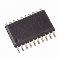
U3741BM-P2FL Atmel, U3741BM-P2FL Datasheet - Page 17

U3741BM-P2FL
Manufacturer Part Number
U3741BM-P2FL
Description
IC RECEIVER PLL 300KHZ 20-SOIC
Manufacturer
Atmel
Datasheet
1.U3741BM-P3FLG3.pdf
(32 pages)
Specifications of U3741BM-P2FL
Frequency
300MHz ~ 450MHz
Sensitivity
-109dBm
Data Rate - Maximum
10 kBaud
Modulation Or Protocol
ASK, FSK
Applications
RKE, Remote Control Systems
Current - Receiving
8.2mA
Data Interface
PCB, Surface Mount
Antenna Connector
PCB, Surface Mount
Voltage - Supply
4.5 V ~ 5.5 V
Operating Temperature
-40°C ~ 105°C
Package / Case
20-SOIC (0.300", 7.50mm Width)
Lead Free Status / RoHS Status
Contains lead / RoHS non-compliant
Features
-
Memory Size
-
Figure 17. Timing Diagram of the OFF Command Via Pin DATA
Figure 18. Timing Diagram of the OFF Command Via Pin ENABLE
Configuration of the
Receiver
4662B–RKE–10/04
data line
DATA (U3741BM)
Serial bi-directional
Out1 (microcontroller)
ENABLE
data line
DATA (U3741BM)
Serial bi-directional
Receiver
on
X
X
X
X
Receiver on
If the receiver is set to polling mode via pin ENABLE, an ‘L’ pulse (T
at that pin. Figure 18 illustrates the timing of that command. After the positive edge of
this pulse, the sleep time T
ENABLE is held to ‘L’. If the receiver is polled exclusively by a microcontroller, T
be programmed to 0 to enable a instantaneous response time. This command is the
faster option than via pin DATA at the cost of an additional connection to the
microcontroller.
The U3741BM receiver is configured via two 12-bit RAM registers called OPMODE and
LIMIT. The registers can be programmed by means of the bi-directional DATA port. If
the register contents have changed due to a voltage drop, this condition is indicated by a
certain output pattern called reset marker (RM). The receiver must be reprogrammed in
that case. After a power-on reset (POR), the registers are set to default mode. If the
receiver is operated in default mode, there is no need to program the registers.
Table 3 on page 18 shows the structure of the registers. According to Table 2 on page
18, bit 1 defines if the receiver is set back to polling mode via the OFF command, (see
section “Receiving Mode” on page 15) or if it is programmed. Bit 2 represents the regis-
ter address. It selects the appropriate register to be programmed.
t1
OFF command
toff
t2
T
Doze
t3
(Start bit)
t4
Bit 1
("1")
t10
t5
t7
Sleep
T
Sleep
elapses. The receiver remains in sleep mode as long as
T
Sleep
Startup mode
X
X
Startup mode
Doze
U3741BM
X
X
) must be issued
Sleep
can
17


