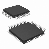
NS16C2752TVSX/NOPB National Semiconductor, NS16C2752TVSX/NOPB Datasheet - Page 21

NS16C2752TVSX/NOPB
Manufacturer Part Number
NS16C2752TVSX/NOPB
Description
IC UART DUAL 64BYTE 48-TQFP
Manufacturer
National Semiconductor
Datasheet
1.NS16C2552TVSXNOPB.pdf
(44 pages)
Specifications of NS16C2752TVSX/NOPB
Features
Programmable
Number Of Channels
2, DUART
Fifo's
64 Byte
Voltage - Supply
2.97 V ~ 5.5 V
With Auto Flow Control
Yes
With Irda Encoder/decoder
Yes
With Modem Control
Yes
Mounting Type
Surface Mount
Package / Case
48-VFQFP
Lead Free Status / RoHS Status
Lead free / RoHS Compliant
Available stocks
Company
Part Number
Manufacturer
Quantity
Price
Company:
Part Number:
NS16C2752TVSX/NOPB
Manufacturer:
Texas Instruments
Quantity:
10 000
Bit
2
1
0
Rx Data Ready
Rx Parity Error
Rx Overrun
Bit Name
Error
R/W
Def
R
R
R
0
0
0
Parity Error Indicator
This bit is the Parity Error (PE) indicator.
1 = Received data word does not have the correct even or odd parity, as selected by the even-
parity-select bit during the character Stop bit time when the character has a parity error.
0 = No parity error (default).
This bit is reset to a logic 0 whenever the CPU reads the contents of the Line Status Register or
when the next valid character is loaded into the Receiver Buffer Register. In the FIFO mode this
error is associated with the particular character in the FIFO it applies to. This error is revealed to
the host when its associated character is at the top of the FIFO.
Overrun Error Indicator
This bit is the Overrun Error (OE) indicator.
This bit indicates that the next character received was transferred into the Receiver Buffer Register
before the CPU could read the previously received character. This transfer overwrites the previous
character. It is reset whenever the CPU reads the contents of the Line Status Register. If the FIFO
mode data continues to fill the FIFO beyond the trigger level, an overrun error will occur only after
the FIFO is full and the next character has been completely received in the shift register. OE is
indicated to the CPU as soon as it happens. The character in the shift register can be overwritten,
but it is not transferred to the FIFO.
1 = Set to a logic 1 during the character stop bit time when the overrun condition exists.
0 = No overrun error (default).
Receiver Data Indicator
This bit is the receiver Data Ready (DR) indicator.
1 = Whenever a complete incoming character has been received and transferred into the Receiver
Buffer Register (RBR) or the FIFO. Bit 0 is reset by reading all of the data in the RBR or the FIFO.
0 = No receive data available (default).
21
Description
www.national.com


