NS16C2752TVSX/NOPB National Semiconductor, NS16C2752TVSX/NOPB Datasheet - Page 34
NS16C2752TVSX/NOPB
Manufacturer Part Number
NS16C2752TVSX/NOPB
Description
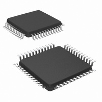
IC UART DUAL 64BYTE 48-TQFP
Manufacturer
National Semiconductor
Datasheet
1.NS16C2552TVSXNOPB.pdf
(44 pages)
Specifications of NS16C2752TVSX/NOPB
Features
Programmable
Number Of Channels
2, DUART
Fifo's
64 Byte
Voltage - Supply
2.97 V ~ 5.5 V
With Auto Flow Control
Yes
With Irda Encoder/decoder
Yes
With Modem Control
Yes
Mounting Type
Surface Mount
Package / Case
48-VFQFP
Lead Free Status / RoHS Status
Lead free / RoHS Compliant
Available stocks
Company
Part Number
Manufacturer
Quantity
Price
Company:

Part Number:
NS16C2752TVSX/NOPB
Manufacturer:
Texas Instruments
Quantity:
10 000


www.national.com
8.0 Design Notes
8.1 DEBUGGING HINTS
Although the UART device is fairly straight forward, there are
cases that when device does not behave as expected. The
normal trouble shooting steps should include the following.
1.
2.
3.
4.
5.
6.
7.
8.2 CLOCK FREQUENCY ACCURACY
In the UART transmission, the transmitter clock and the re-
ceive clock are running in two different clock domains (unlike
in some communication interface that the received clock is a
copy of the transmitter clock by sharing the same clock or by
performing clock-data-recovery). Not only the local oscillator
frequency, but also the clock divisor may introduce error in
between the transmitter and receiver’s baud rate. The ques-
tion is how much error can be tolerated and does not cause
data error?
The UART receiver has an internal sampling clock that is 16X
the data rate. The sampling clock allows data to be sampled
at the 6/16 to 7/16 point of each bit. The following is an ex-
ample of a 8-bit data packet with a start, a parity, and one stop
bit. (Figure 14)
If a receiver baud rate generator deviates from the nominal
baud rate by Δf, where 1/Δf = ΔT, the first sampling point will
deviate from the nominal sample point by 0.5ΔT. Conse-
quently, the second sampling point will deviate by 1.5ΔT, 3rd
will deviate by 2.5ΔT, and the last bit of a packet with L length
(in number of bits) will deviate by
(L − 0.5) x ΔT
In this example, L=11, so that the last bit will deviate by
Check power supply voltage and make sure it is within
the operating range.
Check device pin connections against the datasheet pin
list.
Check an unpopulated printed circuit board (PCB)
against the schematic diagram for any shorts.
Check the device clock input. For oscillator input, the
scope probe can be attached to Xin to verify the clock
voltage swing and frequency. For crystal connection,
attach the scope probe to Xout to check for the oscillation
frequency.
Reset should be active high and normally low.
Use internal loopback mode to test the CPU host
interface. If loopback mode is not working, check the
CPU interface timing including read and write bus timing.
If loopback mode is getting the correct data, check serial
data output and input. The transmit and receive data may
be looped back externally to verify the data path integrity.
FIGURE 14. Nominal Mid-bit Sampling
20204816
34
(11 − 0.5) x ΔT = 10.5ΔT(Figure 15)
Giving some margin for sampling error due to metastability
and jitter assuming that the bit period deviation can not be
more than 6/16 the bit time (i.e., the worst case), 0.375T. So
that
(L − 0.5) x ΔT< 0.375T
for the receiver to correctly recover the transmitted data. Re-
form the equation
ΔT < 0.375T / (L − 0.5)
Using the same example of 11-bit packet (L = 11), at 9600
baud, f = 9600, the sampling clock rate is f (i.e., one sample
per period) and the bit period is
T = 1 / f
ΔT < 0.375T / (L − 0.5) = 0.375 / (f x (L − 0.5))
ΔT < 0.375 / (9600 x 10.5) = 3.7 x 10
The percentage of the deviation from nominal bit period has
to be less than
ΔT / T = (0.375 / (f x (L − 0.5)) x f = 0.375 / L − 0.5)
ΔT / T =3.7 x 10
From the above example, the error percentage increases with
longer packet length (i.e., larger L). The best case is packet
with word length 5, a start bit and a stop bit (L = 7) that is most
tolerant to error.
ΔT / T = 0.375 / (L − 0.5) = 0.375 / 6.5 = 5.8%
The worst case is packet with word length 8, a start bit, a parity
bit, and two stop bits (L = 12) that is least tolerant to error.
ΔT / T = 0.375 / L − 0.5) = 0.375 / 11.5 = 3.2%
8.3 CRYSTAL REQUIREMENTS
The crystal used should meet the following requirements.
1.
2.
3.
4.
AT cut with parallel resonance.
Fundamental oscillation mode between 1 to 24 MHz.
Frequency tolerance and drift is well within the UART
application requirements, and they are not a concern.
The load capacitance of the crystal should match the load
capacitance of the oscillator circuitry seen by the crystal.
Under the AC conditions, the oscillator load capacitance
is a lump sum of parasitic capacitance and external
capacitors. The capacitances connecting to oscillator
input and output are in series seen by the crystal. (Figure
16.) External capacitors, C1 and C2, are not required to
be very accurate. The best practice to follow crystal
manufacturer’s recommendation for the load
capacitance value.
FIGURE 15. Deviated Baud Rate Sampling
-6
x 9600 = 3.6%
-6
(sec) or 3.7 µs.
20204817
Related parts for NS16C2752TVSX/NOPB
Image
Part Number
Description
Manufacturer
Datasheet
Request
R

Part Number:
Description:
National Semiconductor [8-Bit D/A Converter]
Manufacturer:
National Semiconductor
Datasheet:
Part Number:
Description:
National Semiconductor [Media Coprocessor]
Manufacturer:
National Semiconductor
Datasheet:
Part Number:
Description:
Digitally Controlled Tone and Volume Circuit with Stereo Audio Power Amplifier, Microphone Preamp Stage and National 3D Sound
Manufacturer:
National Semiconductor
Datasheet:
Part Number:
Description:
Digitally Controlled Tone and Volume Circuit with Stereo Audio Power Amplifier, Microphone Preamp Stage and National 3D Sound
Manufacturer:
National Semiconductor
Datasheet:
Part Number:
Description:
AC97 Rev 2 Codec with Sample Rate Conversion and National 3D Sound
Manufacturer:
National Semiconductor
Part Number:
Description:
Manufacturer:
National Semiconductor
Datasheet:
Part Number:
Description:
Manufacturer:
National Semiconductor
Datasheet:
Part Number:
Description:
General Purpose, Low Voltage, Low Power, Rail-to-Rail Output Operational Amplifiers
Manufacturer:
National Semiconductor
Datasheet:
Part Number:
Description:
8-bit 20 MSPS flash A/D converter.
Manufacturer:
National Semiconductor
Datasheet:
Part Number:
Description:
Low Noise Quad Operational Amplifier
Manufacturer:
National Semiconductor
Datasheet:
Part Number:
Description:
Quad Differential Line Receivers
Manufacturer:
National Semiconductor
Datasheet:
Part Number:
Description:
Quad High Speed Trapezoidal? Bus Transceiver
Manufacturer:
National Semiconductor
Datasheet:
Part Number:
Description:
Dual Line Receiver
Manufacturer:
National Semiconductor
Datasheet:
Part Number:
Description:
TTL to 10k ECL Level Translator with Latch
Manufacturer:
National Semiconductor
Datasheet: