NS16C2752TVSX/NOPB National Semiconductor, NS16C2752TVSX/NOPB Datasheet - Page 7
NS16C2752TVSX/NOPB
Manufacturer Part Number
NS16C2752TVSX/NOPB
Description
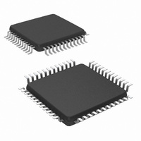
IC UART DUAL 64BYTE 48-TQFP
Manufacturer
National Semiconductor
Datasheet
1.NS16C2552TVSXNOPB.pdf
(44 pages)
Specifications of NS16C2752TVSX/NOPB
Features
Programmable
Number Of Channels
2, DUART
Fifo's
64 Byte
Voltage - Supply
2.97 V ~ 5.5 V
With Auto Flow Control
Yes
With Irda Encoder/decoder
Yes
With Modem Control
Yes
Mounting Type
Surface Mount
Package / Case
48-VFQFP
Lead Free Status / RoHS Status
Lead free / RoHS Compliant
Available stocks
Company
Part Number
Manufacturer
Quantity
Price
Company:

Part Number:
NS16C2752TVSX/NOPB
Manufacturer:
Texas Instruments
Quantity:
10 000


DCD1
DCD2
RI1
RI2
MF1
MF2
Signal
Name
Type
O
I
I
PLCC
Pin #
42
30
43
31
35
19
TQFP
Pin #
40
26
41
27
32
14
UART Data-carrier-detect:
When low, DCD indicates that the data carrier has been detected by the remote link partner.
The DCD signal is a MODEM status input and can be read for the appropriate channel in MSR
[7]. This bit reflects the complement of the DCD signal. MSR[3] indicates if the DCD input has
changed state since the previous reading of the MODEM Status Register. DCD has no effect
on the receiver.
Note: Whenever the DCD bit of the MSR changes state, an interrupt is generated if the MODEM Status Interrupt is
UART Ring-detector:
When low, RI indicates that a telephone ringing is active. The RI signal is a MODEM status
input and can be read for the appropriate channel in MSR[6]. This bit reflects the complement
of the RI signal. MSR[2] indicates whether the RI input signal has changed state from low to
high since the previous reading of the MSR.
Note: Whenever the RI bit of the MSR changes from a high to a low state, an interrupt is generated if the MODEM
UART Multi-function Pin:
MF can be programmed for any one of three signal functions OUT2, BAUDOUT or RXRDY.
Bits 2 and 1 of the Alternate Function Register select which output signal will be present on this
pin. OUT2 is the default signal and it is selected immediately after master reset or power-up.
The OUT2 can be set active low by programming bit 3 (OUT2) of the MCR to a logic 1. A Master
Reset operation sets this signal to its inactive (high) state. Loop Mode holds this signal in its
inactive state.
The BAUDOUT signal is the 16X clock output that drives the transmitter and receiver logic of
the associated serial channel. This signal is the result of the XIN clock divided by the value in
the Divisor Latch Registers. The BAUDOUT signal for each channel is internally connected to
provide the receiver clock (formerly RCLK on the PC16550D).
The RXRDY signal can be used to request a DMA transfer of data from the RCVR FIFO. Details
regarding the active and inactive states of this signal are described in Section 6.5 FIFO
CONTROL REGISTER (FCR) and Section 7.9 DMA OPERATION.
enabled.
Status Interrupt is enabled.
7
Description
www.national.com
Related parts for NS16C2752TVSX/NOPB
Image
Part Number
Description
Manufacturer
Datasheet
Request
R

Part Number:
Description:
National Semiconductor [8-Bit D/A Converter]
Manufacturer:
National Semiconductor
Datasheet:
Part Number:
Description:
National Semiconductor [Media Coprocessor]
Manufacturer:
National Semiconductor
Datasheet:
Part Number:
Description:
Digitally Controlled Tone and Volume Circuit with Stereo Audio Power Amplifier, Microphone Preamp Stage and National 3D Sound
Manufacturer:
National Semiconductor
Datasheet:
Part Number:
Description:
Digitally Controlled Tone and Volume Circuit with Stereo Audio Power Amplifier, Microphone Preamp Stage and National 3D Sound
Manufacturer:
National Semiconductor
Datasheet:
Part Number:
Description:
AC97 Rev 2 Codec with Sample Rate Conversion and National 3D Sound
Manufacturer:
National Semiconductor
Part Number:
Description:
Manufacturer:
National Semiconductor
Datasheet:
Part Number:
Description:
Manufacturer:
National Semiconductor
Datasheet:
Part Number:
Description:
General Purpose, Low Voltage, Low Power, Rail-to-Rail Output Operational Amplifiers
Manufacturer:
National Semiconductor
Datasheet:
Part Number:
Description:
8-bit 20 MSPS flash A/D converter.
Manufacturer:
National Semiconductor
Datasheet:
Part Number:
Description:
Low Noise Quad Operational Amplifier
Manufacturer:
National Semiconductor
Datasheet:
Part Number:
Description:
Quad Differential Line Receivers
Manufacturer:
National Semiconductor
Datasheet:
Part Number:
Description:
Quad High Speed Trapezoidal? Bus Transceiver
Manufacturer:
National Semiconductor
Datasheet:
Part Number:
Description:
Dual Line Receiver
Manufacturer:
National Semiconductor
Datasheet:
Part Number:
Description:
TTL to 10k ECL Level Translator with Latch
Manufacturer:
National Semiconductor
Datasheet: