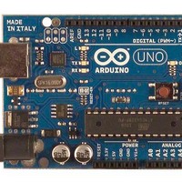
A000046 Arduino, A000046 Datasheet - Page 134
A000046
Manufacturer Part Number
A000046
Description
MCU, MPU & DSP Development Tools Uno
Manufacturer
Arduino
Series
-r
Type
MCUr
Specifications of A000046
Processor To Be Evaluated
ATmega328
Interface Type
USB, I2C, SPI
Dimensions
2.7 in x 2.1 in
Operating Supply Voltage
5 V
Contents
Board
Lead Free Status / RoHS Status
Lead free / RoHS Compliant
For Use With/related Products
ATmega328


15.11 Register Description
15.11.1
8161D–AVR–10/09
TCCR1A – Timer/Counter1 Control Register A
Figure 15-13
Figure 15-13. Timer/Counter Timing Diagram, with Prescaler (f
• Bit 7:6 – COM1A1:0: Compare Output Mode for Channel A
• Bit 5:4 – COM1B1:0: Compare Output Mode for Channel B
The COM1A1:0 and COM1B1:0 control the Output Compare pins (OC1A and OC1B respec-
tively) behavior. If one or both of the COM1A1:0 bits are written to one, the OC1A output
overrides the normal port functionality of the I/O pin it is connected to. If one or both of the
COM1B1:0 bit are written to one, the OC1B output overrides the normal port functionality of the
I/O pin it is connected to. However, note that the Data Direction Register (DDR) bit correspond-
ing to the OC1A or OC1B pin must be set in order to enable the output driver.
When the OC1A or OC1B is connected to the pin, the function of the COM1x1:0 bits is depen-
dent of the WGM13:0 bits setting.
WGM13:0 bits are set to a Normal or a CTC mode (non-PWM).
Table 15-1.
Bit
(0x80)
Read/Write
Initial Value
COM1A1/COM1B1
and ICF n
(PC and PFC PWM)
TOVn
(CTC and FPWM)
(Update at TOP)
0
0
1
1
OCRnx
TCNTn
TCNTn
as TOP)
(clk
clk
clk
I/O
(FPWM)
shows the same timing data, but with the prescaler enabled.
I/O
Tn
/8)
COM1A1
(if used
Compare Output Mode, non-PWM
R/W
7
0
COM1A0
COM1A0/COM1B0
R/W
6
0
TOP - 1
TOP - 1
Old OCRnx Value
0
1
0
1
COM1B1
ATmega48PA/88PA/168PA/328P
R/W
Table 15-1
5
0
COM1B0
R/W
4
0
Description
Normal port operation, OC1A/OC1B disconnected.
Toggle OC1A/OC1B on Compare Match.
Clear OC1A/OC1B on Compare Match (Set output to
low level).
Set OC1A/OC1B on Compare Match (Set output to
high level).
shows the COM1x1:0 bit functionality when the
TOP
TOP
R
3
0
–
BOTTOM
TOP - 1
clk_I/O
R
2
0
–
New OCRnx Value
/8)
WGM11
R/W
1
0
BOTTOM + 1
TOP - 2
WGM10
R/W
0
0
TCCR1A
134
Related parts for A000046
Image
Part Number
Description
Manufacturer
Datasheet
Request
R

Part Number:
Description:
Daughter Cards & OEM Boards ARDUINO UNO PROTO PCB REV 3
Manufacturer:
Arduino
Part Number:
Description:
Daughter Cards & OEM Boards ARDUINO SHIELD PROTO KIT REV 3
Manufacturer:
Arduino
Part Number:
Description:
Daughter Cards & OEM Boards ARDUINO MEGA PROTO KIT REV 3
Manufacturer:
Arduino
Part Number:
Description:
Daughter Cards & OEM Boards ARDUINO MEGA PROTO PCB REV 3
Manufacturer:
Arduino
Part Number:
Description:
Development Boards & Kits - AVR ARDUINO STARTER KIT W/ UNO REV3
Manufacturer:
Arduino
Part Number:
Description:
RF Development Tools ARDUINO SHIELD WIRELESS PROTO
Manufacturer:
Arduino
Datasheet:
Part Number:
Description:
RF Development Tools ARDUINO SHIELD WIRELESS WITH SD
Manufacturer:
Arduino
Datasheet:

Part Number:
Description:
Development Software Getting started w/Arduino
Manufacturer:
Arduino

Part Number:
Description:
Ethernet Modules & Development Tools Ethernet Shield for Arduino
Manufacturer:
Arduino

Part Number:
Description:
MCU, MPU & DSP Development Tools LilyPad Arduino Main Board
Manufacturer:
Arduino

Part Number:
Description:
ARDUINO NANO Board
Manufacturer:
Arduino
Datasheet:
Part Number:
Description:
Ethernet Modules & Development Tools ETHERNET SHEILD PoE FOR ARDUINO
Manufacturer:
Arduino
Datasheet:

Part Number:
Description:
ATMEGA328 MCU IC W/ Arduino UNO Bootloader
Manufacturer:
Arduino
Datasheet:
Part Number:
Description:
Memory Cards MICRO SD CARD 1GB WITH SD ADAPTER
Manufacturer:
Arduino