A000046 Arduino, A000046 Datasheet - Page 250
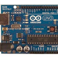
A000046
Manufacturer Part Number
A000046
Description
MCU, MPU & DSP Development Tools Uno
Manufacturer
Arduino
Series
-r
Type
MCUr
Specifications of A000046
Processor To Be Evaluated
ATmega328
Interface Type
USB, I2C, SPI
Dimensions
2.7 in x 2.1 in
Operating Supply Voltage
5 V
Contents
Board
Lead Free Status / RoHS Status
Lead free / RoHS Compliant
For Use With/related Products
ATmega328


23. Analog-to-Digital Converter
23.1
23.2
8161D–AVR–10/09
Features
Overview
•
•
•
•
•
•
•
•
•
•
•
•
•
•
The ATmega48PA/88PA/168PA/328P features a 10-bit successive approximation ADC. The
ADC is connected to an 8-channel Analog Multiplexer which allows eight single-ended voltage
inputs constructed from the pins of Port A. The single-ended voltage inputs refer to 0V (GND).
The ADC contains a Sample and Hold circuit which ensures that the input voltage to the ADC is
held at a constant level during conversion. A block diagram of the ADC is shown in
on page
The ADC has a separate analog supply voltage pin, AV
from V
Internal reference voltages of nominally 1.1V or AV
ence may be externally decoupled at the AREF pin by a capacitor for better noise performance.
The Power Reduction ADC bit, PRADC, in
be disabled by writing a logical zero to enable the ADC.
The ADC converts an analog input voltage to a 10-bit digital value through successive approxi-
mation. The minimum value represents GND and the maximum value represents the voltage on
the AREF pin minus 1 LSB. Optionally, AV
nected to the AREF pin by writing to the REFSn bits in the ADMUX Register. The internal
voltage reference may thus be decoupled by an external capacitor at the AREF pin to improve
noise immunity.
10-bit Resolution
0.5 LSB Integral Non-linearity
± 2 LSB Absolute Accuracy
13 - 260 µs Conversion Time
Up to 76.9 kSPS (Up to 15 kSPS at Maximum Resolution)
6 Multiplexed Single Ended Input Channels
2 Additional Multiplexed Single Ended Input Channels (TQFP and QFN/MLF Package only)
Temperature Sensor Input Channel
Optional Left Adjustment for ADC Result Readout
0 - V
Selectable 1.1V ADC Reference Voltage
Free Running or Single Conversion Mode
Interrupt on ADC Conversion Complete
Sleep Mode Noise Canceler
CC
CC
251.
ADC Input Voltage Range
. See the paragraph
”ADC Noise Canceler” on page 256
ATmega48PA/88PA/168PA/328P
CC
”Minimizing Power Consumption” on page 42
or an internal 1.1V reference voltage may be con-
CC
CC
are provided On-chip. The voltage refer-
. AV
CC
must not differ more than ±0.3V
on how to connect this pin.
Figure 23-1
must
250
Related parts for A000046
Image
Part Number
Description
Manufacturer
Datasheet
Request
R

Part Number:
Description:
Daughter Cards & OEM Boards ARDUINO UNO PROTO PCB REV 3
Manufacturer:
Arduino
Part Number:
Description:
Daughter Cards & OEM Boards ARDUINO SHIELD PROTO KIT REV 3
Manufacturer:
Arduino
Part Number:
Description:
Daughter Cards & OEM Boards ARDUINO MEGA PROTO KIT REV 3
Manufacturer:
Arduino
Part Number:
Description:
Daughter Cards & OEM Boards ARDUINO MEGA PROTO PCB REV 3
Manufacturer:
Arduino
Part Number:
Description:
Development Boards & Kits - AVR ARDUINO STARTER KIT W/ UNO REV3
Manufacturer:
Arduino
Part Number:
Description:
RF Development Tools ARDUINO SHIELD WIRELESS PROTO
Manufacturer:
Arduino
Datasheet:
Part Number:
Description:
RF Development Tools ARDUINO SHIELD WIRELESS WITH SD
Manufacturer:
Arduino
Datasheet:

Part Number:
Description:
Development Software Getting started w/Arduino
Manufacturer:
Arduino

Part Number:
Description:
Ethernet Modules & Development Tools Ethernet Shield for Arduino
Manufacturer:
Arduino

Part Number:
Description:
MCU, MPU & DSP Development Tools LilyPad Arduino Main Board
Manufacturer:
Arduino

Part Number:
Description:
ARDUINO NANO Board
Manufacturer:
Arduino
Datasheet:
Part Number:
Description:
Ethernet Modules & Development Tools ETHERNET SHEILD PoE FOR ARDUINO
Manufacturer:
Arduino
Datasheet:

Part Number:
Description:
ATMEGA328 MCU IC W/ Arduino UNO Bootloader
Manufacturer:
Arduino
Datasheet:
Part Number:
Description:
Memory Cards MICRO SD CARD 1GB WITH SD ADAPTER
Manufacturer:
Arduino