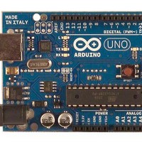
A000046 Arduino, A000046 Datasheet - Page 83
A000046
Manufacturer Part Number
A000046
Description
MCU, MPU & DSP Development Tools Uno
Manufacturer
Arduino
Series
-r
Type
MCUr
Specifications of A000046
Processor To Be Evaluated
ATmega328
Interface Type
USB, I2C, SPI
Dimensions
2.7 in x 2.1 in
Operating Supply Voltage
5 V
Contents
Board
Lead Free Status / RoHS Status
Lead free / RoHS Compliant
For Use With/related Products
ATmega328


ATmega48PA/88PA/168PA/328P
AS2 bit in ASSR is set (one) to enable asynchronous clocking of Timer/Counter2, pin PB6 is dis-
connected from the port, and becomes the input of the inverting Oscillator amplifier. In this
mode, a crystal Oscillator is connected to this pin, and the pin can not be used as an I/O pin.
PCINT6: Pin Change Interrupt source 6. The PB6 pin can serve as an external interrupt source.
If PB6 is used as a clock pin, DDB6, PORTB6 and PINB6 will all read 0.
• SCK/PCINT5 – Port B, Bit 5
SCK: Master Clock output, Slave Clock input pin for SPI channel. When the SPI is enabled as a
Slave, this pin is configured as an input regardless of the setting of DDB5. When the SPI is
enabled as a Master, the data direction of this pin is controlled by DDB5. When the pin is forced
by the SPI to be an input, the pull-up can still be controlled by the PORTB5 bit.
PCINT5: Pin Change Interrupt source 5. The PB5 pin can serve as an external interrupt source.
• MISO/PCINT4 – Port B, Bit 4
MISO: Master Data input, Slave Data output pin for SPI channel. When the SPI is enabled as a
Master, this pin is configured as an input regardless of the setting of DDB4. When the SPI is
enabled as a Slave, the data direction of this pin is controlled by DDB4. When the pin is forced
by the SPI to be an input, the pull-up can still be controlled by the PORTB4 bit.
PCINT4: Pin Change Interrupt source 4. The PB4 pin can serve as an external interrupt source.
• MOSI/OC2/PCINT3 – Port B, Bit 3
MOSI: SPI Master Data output, Slave Data input for SPI channel. When the SPI is enabled as a
Slave, this pin is configured as an input regardless of the setting of DDB3. When the SPI is
enabled as a Master, the data direction of this pin is controlled by DDB3. When the pin is forced
by the SPI to be an input, the pull-up can still be controlled by the PORTB3 bit.
OC2, Output Compare Match Output: The PB3 pin can serve as an external output for the
Timer/Counter2 Compare Match. The PB3 pin has to be configured as an output (DDB3 set
(one)) to serve this function. The OC2 pin is also the output pin for the PWM mode timer
function.
PCINT3: Pin Change Interrupt source 3. The PB3 pin can serve as an external interrupt source.
• SS/OC1B/PCINT2 – Port B, Bit 2
SS: Slave Select input. When the SPI is enabled as a Slave, this pin is configured as an input
regardless of the setting of DDB2. As a Slave, the SPI is activated when this pin is driven low.
When the SPI is enabled as a Master, the data direction of this pin is controlled by DDB2. When
the pin is forced by the SPI to be an input, the pull-up can still be controlled by the PORTB2 bit.
OC1B, Output Compare Match output: The PB2 pin can serve as an external output for the
Timer/Counter1 Compare Match B. The PB2 pin has to be configured as an output (DDB2 set
(one)) to serve this function. The OC1B pin is also the output pin for the PWM mode timer
function.
PCINT2: Pin Change Interrupt source 2. The PB2 pin can serve as an external interrupt source.
• OC1A/PCINT1 – Port B, Bit 1
OC1A, Output Compare Match output: The PB1 pin can serve as an external output for the
Timer/Counter1 Compare Match A. The PB1 pin has to be configured as an output (DDB1 set
83
8161D–AVR–10/09
Related parts for A000046
Image
Part Number
Description
Manufacturer
Datasheet
Request
R

Part Number:
Description:
Daughter Cards & OEM Boards ARDUINO UNO PROTO PCB REV 3
Manufacturer:
Arduino
Part Number:
Description:
Daughter Cards & OEM Boards ARDUINO SHIELD PROTO KIT REV 3
Manufacturer:
Arduino
Part Number:
Description:
Daughter Cards & OEM Boards ARDUINO MEGA PROTO KIT REV 3
Manufacturer:
Arduino
Part Number:
Description:
Daughter Cards & OEM Boards ARDUINO MEGA PROTO PCB REV 3
Manufacturer:
Arduino
Part Number:
Description:
Development Boards & Kits - AVR ARDUINO STARTER KIT W/ UNO REV3
Manufacturer:
Arduino
Part Number:
Description:
RF Development Tools ARDUINO SHIELD WIRELESS PROTO
Manufacturer:
Arduino
Datasheet:
Part Number:
Description:
RF Development Tools ARDUINO SHIELD WIRELESS WITH SD
Manufacturer:
Arduino
Datasheet:

Part Number:
Description:
Development Software Getting started w/Arduino
Manufacturer:
Arduino

Part Number:
Description:
Ethernet Modules & Development Tools Ethernet Shield for Arduino
Manufacturer:
Arduino

Part Number:
Description:
MCU, MPU & DSP Development Tools LilyPad Arduino Main Board
Manufacturer:
Arduino

Part Number:
Description:
ARDUINO NANO Board
Manufacturer:
Arduino
Datasheet:
Part Number:
Description:
Ethernet Modules & Development Tools ETHERNET SHEILD PoE FOR ARDUINO
Manufacturer:
Arduino
Datasheet:

Part Number:
Description:
ATMEGA328 MCU IC W/ Arduino UNO Bootloader
Manufacturer:
Arduino
Datasheet:
Part Number:
Description:
Memory Cards MICRO SD CARD 1GB WITH SD ADAPTER
Manufacturer:
Arduino