A000046 Arduino, A000046 Datasheet - Page 75
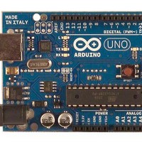
A000046
Manufacturer Part Number
A000046
Description
MCU, MPU & DSP Development Tools Uno
Manufacturer
Arduino
Series
-r
Type
MCUr
Specifications of A000046
Processor To Be Evaluated
ATmega328
Interface Type
USB, I2C, SPI
Dimensions
2.7 in x 2.1 in
Operating Supply Voltage
5 V
Contents
Board
Lead Free Status / RoHS Status
Lead free / RoHS Compliant
For Use With/related Products
ATmega328


13. I/O-Ports
13.1
8161D–AVR–10/09
Overview
All AVR ports have true Read-Modify-Write functionality when used as general digital I/O ports.
This means that the direction of one port pin can be changed without unintentionally changing
the direction of any other pin with the SBI and CBI instructions. The same applies when chang-
ing drive value (if configured as output) or enabling/disabling of pull-up resistors (if configured as
input). Each output buffer has symmetrical drive characteristics with both high sink and source
capability. The pin driver is strong enough to drive LED displays directly. All port pins have indi-
vidually selectable pull-up resistors with a supply-voltage invariant resistance. All I/O pins have
protection diodes to both V
acteristics” on page 313
Figure 13-1. I/O Pin Equivalent Schematic
All registers and bit references in this section are written in general form. A lower case “x” repre-
sents the numbering letter for the port, and a lower case “n” represents the bit number. However,
when using the register or bit defines in a program, the precise form must be used. For example,
PORTB3 for bit no. 3 in Port B, here documented generally as PORTxn. The physical I/O Regis-
ters and bit locations are listed in
Three I/O memory address locations are allocated for each port, one each for the Data Register
– PORTx, Data Direction Register – DDRx, and the Port Input Pins – PINx. The Port Input Pins
I/O location is read only, while the Data Register and the Data Direction Register are read/write.
However, writing a logic one to a bit in the PINx Register, will result in a toggle in the correspond-
ing bit in the Data Register. In addition, the Pull-up Disable – PUD bit in MCUCR disables the
pull-up function for all pins in all ports when set.
Using the I/O port as General Digital I/O is described in
76. Most port pins are multiplexed with alternate functions for the peripheral features on the
device. How each alternate function interferes with the port pin is described in
Functions” on page
nate functions.
Pxn
80. Refer to the individual module sections for a full description of the alter-
for a complete list of parameters.
CC
and Ground as indicated in
”Register Description” on page
C
ATmega48PA/88PA/168PA/328P
pin
”Ports as General Digital I/O” on page
Figure
"General Digital I/O" for
92.
13-1. Refer to
See Figure
R
Details
pu
Logic
”Electrical Char-
”Alternate Port
75
Related parts for A000046
Image
Part Number
Description
Manufacturer
Datasheet
Request
R

Part Number:
Description:
Daughter Cards & OEM Boards ARDUINO UNO PROTO PCB REV 3
Manufacturer:
Arduino
Part Number:
Description:
Daughter Cards & OEM Boards ARDUINO SHIELD PROTO KIT REV 3
Manufacturer:
Arduino
Part Number:
Description:
Daughter Cards & OEM Boards ARDUINO MEGA PROTO KIT REV 3
Manufacturer:
Arduino
Part Number:
Description:
Daughter Cards & OEM Boards ARDUINO MEGA PROTO PCB REV 3
Manufacturer:
Arduino
Part Number:
Description:
Development Boards & Kits - AVR ARDUINO STARTER KIT W/ UNO REV3
Manufacturer:
Arduino
Part Number:
Description:
RF Development Tools ARDUINO SHIELD WIRELESS PROTO
Manufacturer:
Arduino
Datasheet:
Part Number:
Description:
RF Development Tools ARDUINO SHIELD WIRELESS WITH SD
Manufacturer:
Arduino
Datasheet:

Part Number:
Description:
Development Software Getting started w/Arduino
Manufacturer:
Arduino

Part Number:
Description:
Ethernet Modules & Development Tools Ethernet Shield for Arduino
Manufacturer:
Arduino

Part Number:
Description:
MCU, MPU & DSP Development Tools LilyPad Arduino Main Board
Manufacturer:
Arduino

Part Number:
Description:
ARDUINO NANO Board
Manufacturer:
Arduino
Datasheet:
Part Number:
Description:
Ethernet Modules & Development Tools ETHERNET SHEILD PoE FOR ARDUINO
Manufacturer:
Arduino
Datasheet:

Part Number:
Description:
ATMEGA328 MCU IC W/ Arduino UNO Bootloader
Manufacturer:
Arduino
Datasheet:
Part Number:
Description:
Memory Cards MICRO SD CARD 1GB WITH SD ADAPTER
Manufacturer:
Arduino