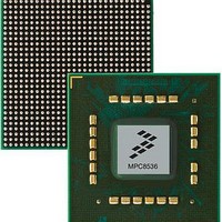
MPC8536BVTATH Freescale Semiconductor, MPC8536BVTATH Datasheet - Page 48

MPC8536BVTATH
Manufacturer Part Number
MPC8536BVTATH
Description
Microprocessors (MPU) 8536 INDUSTRIAL 1250
Manufacturer
Freescale Semiconductor
Datasheet
1.MPC8536EBVTAQG.pdf
(126 pages)
Specifications of MPC8536BVTATH
Processor Series
MPC85xx
Core
e500
Data Bus Width
32 bit
Maximum Clock Frequency
1250 MHz
Operating Supply Voltage
3.3 V
Maximum Operating Temperature
+ 105 C
Mounting Style
SMD/SMT
Interface Type
I2C, SPI, UART
Minimum Operating Temperature
0 C
Package / Case
FCPBGA-783
Lead Free Status / RoHS Status
Lead free / RoHS Compliant
Available stocks
Company
Part Number
Manufacturer
Quantity
Price
Company:
Part Number:
MPC8536BVTATHA
Manufacturer:
Freescale Semiconductor
Quantity:
10 000
Ethernet: Enhanced Three-Speed Ethernet (eTSEC), MII Management
Figure 22
2.9.2.4.2
Table 33
48
At recommended operating conditions with L/TV
Clock period for TBI Receive Clock 0, 1
Skew for TBI Receive Clock 0, 1
Duty cycle for TBI Receive Clock 0, 1
RCG[9:0] setup time to rising edge of TBI Receive Clock 0, 1
RCG[9:0] hold time to rising edge of TBI Receive Clock 0, 1
Clock rise time (20%-80%) for TBI Receive Clock 0, 1
Clock fall time (80%-20%) for TBI Receive Clock 0, 1
Note:
1. The symbols used for timing specifications herein follow the pattern of t
2. The signals “TBI Receive Clock 0” and “TBI Receive Clock 1” refer to TSECn_RX_CLK and TSECn_TX_CLK pins
(reference)(state)
symbolizes TBI receive timing (TR) with respect to the time data input signals (D) reach the valid state (V) relative to the
t
respect to the time data input signals (D) went invalid (X) relative to the t
state. Note that, in general, the clock reference symbol representation is based on three letters representing the clock of
a particular functional. For example, the subscript of t
the latter convention is used with the appropriate letter: R (rise) or F (fall). For symbols representing skews, the subscript
is skew (SK) followed by the clock that is being skewed (TRX).
respectively. These two clock signals are also referred as PMA_RX_CLK[0:1].
TRX
provides the TBI receive AC timing specifications.
clock reference (K) going to the high (H) state or setup time. Also, t
shows the TBI transmit AC timing diagram.
TBI Receive AC Timing Specifications
GTX_CLK
TCG[9:0]
for inputs and t
MPC8535E PowerQUICC III Integrated Processor Hardware Specifications, Rev. 3
Parameter/Condition
(first two letters of functional block)(reference)(state)(signal)(state)
Table 33. TBI Receive AC Timing Specifications
Figure 22. TBI Transmit AC Timing Diagram
t
TTXH
t
TTKHDV
t
DD
TTXF
2
of 3.3 V ± 5%.
t
TTX
TRX
represents the TBI (T) receive (RX) clock. For rise and fall times,
t
t
TTXF
Symbol
TRXH
t
t
TRDVKH
TRDXKH
t
t
SKTRX
t
TRXR
t
TRXF
TRX
/t
TRX
1
TRDXKH
t
(first two letters of functional block)(signal)(state)
TTKHDX
TRX
t
TTXR
clock reference (K) going to the high (H)
Min
7.5
2.5
1.5
0.7
0.7
40
—
symbolizes TBI receive timing (TR) with
for outputs. For example, t
t
TTXR
16.0
Typ
—
—
—
—
—
—
Freescale Semiconductor
Max
8.5
2.4
2.4
60
—
—
—
TRDVKH
Unit
ns
ns
ns
ns
ns
ns
%


