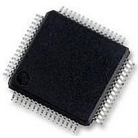
SAF-XC878CM-16FFI Infineon Technologies, SAF-XC878CM-16FFI Datasheet - Page 110

SAF-XC878CM-16FFI
Manufacturer Part Number
SAF-XC878CM-16FFI
Description
MCU, 8BIT, 64K FLASH, 5V, 64LQFP
Manufacturer
Infineon Technologies
Datasheet
1.SAF-XC878CM-16FFI.pdf
(146 pages)
Specifications of SAF-XC878CM-16FFI
Controller Family/series
XC800
Core Size
8bit
Program Memory Size
64KB
Ram Memory Size
3328Byte
No. Of Timers
4
No. Of Pwm Channels
10
Digital Ic Case Style
LQFP
Supply Voltage Range
4.5V To
Peripherals
ADC, PWM, Timer
Rohs Compliant
Yes
Lead Free Status / RoHS Status
Lead free / RoHS Compliant
Available stocks
Company
Part Number
Manufacturer
Quantity
Price
Company:
Part Number:
SAF-XC878CM-16FFI 3V3 AA
Manufacturer:
Infineon Technologies
Quantity:
10 000
Company:
Part Number:
SAF-XC878CM-16FFI 3V3 AC
Manufacturer:
Infineon Technologies
Quantity:
10 000
Company:
Part Number:
SAF-XC878CM-16FFI 5V AA
Manufacturer:
Infineon Technologies
Quantity:
10 000
Part Number:
SAF-XC878CM-16FFI 5V AA
Manufacturer:
INFINEON/英飞凌
Quantity:
20 000
Company:
Part Number:
SAF-XC878CM-16FFI 5V AC
Manufacturer:
Infineon Technologies
Quantity:
10 000
Part Number:
SAF-XC878CM-16FFI5VAC
Manufacturer:
INFINEON/英飞凌
Quantity:
20 000
3.22
The XC878 includes a high-performance 10-bit Analog-to-Digital Converter (ADC) with
eight multiplexed analog input channels. The ADC uses a successive approximation
technique to convert the analog voltage levels from up to eight different sources. The
analog input channels of the ADC are available at AN0 - AN7.
Features
•
•
•
•
•
•
•
•
•
•
•
•
•
•
•
•
•
•
3.22.1
A common module clock
digital parts of the ADC module:
•
•
•
Figure 30
selected by bit field CTC in register GLOBCTR. A prescaling ratio of 32 can be selected
when the maximum performance of the ADC is not required.
Data Sheet
Successive approximation
8-bit or 10-bit resolution
Eight analog channels
Four independent result registers
Result data protection for slow CPU access
(wait-for-read mode)
Single conversion mode
Autoscan functionality
Limit checking for conversion results
Data reduction filter
(accumulation of up to 2 conversion results)
Two independent conversion request sources with programmable priority
Selectable conversion request trigger
Flexible interrupt generation with configurable service nodes
Programmable sample time
Programmable clock divider
Cancel/restart feature for running conversions
Integrated sample and hold circuitry
Compensation of offset errors
Low power modes
f
f
and the sample time). This clock is generated internally in the analog part, based on
the input clock
f
ADCA
ADCI
ADCD
is internal clock for the analog part (defines the time base for conversion length
is input clock for the analog part.
is input clock for the digital part.
shows the clocking scheme of the ADC module. The prescaler ratio is
Analog-to-Digital Converter
ADC Clocking Scheme
f
ADCA
to generate a correct duty cycle for the analog components.
f
ADC
generates the various clock signals used by the analog and
101
Functional Description
XC878CLM
V1.2, 2009-11


