LMR4769EW-WCB DENSITRON, LMR4769EW-WCB Datasheet - Page 14
LMR4769EW-WCB
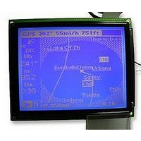
Manufacturer Part Number
LMR4769EW-WCB
Description
LCD MODULE, 240X320, BLUE
Manufacturer
DENSITRON
Datasheet
1.LMR4769EW-WCB.pdf
(108 pages)
Specifications of LMR4769EW-WCB
Lcd Display Type
STN
Pixel Size (h X W)
0.34mm X 0.34mm
Display Mode
Transflective
Interface Type
Serial
Viewing Area (h X W)
92.14mm X 120.14mm
Supply Voltage
32V
External Depth
15.6mm
External
RoHS Compliant
Svhc
No SVHC (15-Dec-2010)
Rohs Compliant
Yes
Backlighting Colour
Blue
Pixel Pitch (h X W)
0.36mm X 0.36mm


2.2
2.2.1
2.2.2
S1D13700 Technical Manual
Note 1: Because the spike power supply current in the S1D13700 could reach levels that are several
Note 2: Because the external clock fed in from the CLKI pin is needed to internally generate the
COREVDD
Pin Name
HIOVDD
NIOVDD
Pin Functions
XCG1
XCD1
CNF0
CNF1
CLKI
V
Power Supply Pins
Oscillator and Clock Input Pins
SS
tens higher than the average amount of dynamically consumed current, measures must be
taken to minimize the power supply impedance of the S1D13700. For example, use thick
power supply wiring from the power supply to the S1D13700 or insert a capacitor of 0.47 mF or
more (with good frequency characteristics) between V
These measures will help to reduce power supply impedance.
fundamental timing in the S1D13700, the oscillation characteristic requirements given in
Section 5.4.3 “External Clock Input Characteristics” on page 92 must be met.
Power supply for host interface I/O drive. Connect a 5 V or 3.3 V power supply to this pin. (Shared
with MPU power supply pin, V
Power supply for LCD I/O drive other than host of interface I/O. Connect a 5 V or 3.3 V power supply
to this pin.
Power supply for internal logic. Connect a 3.3 V power supply to this pin.
Connects to 0 V earth ground (GND).
Generally used as the input clock source for the bus and memory clocks.
These pins are used to connect a crystal resonator for the internal clock-generating oscillator. For
details, see Section 4.2 “Oscillator Circuit” on page 70. To use the external clock (fed in from the
CLKI pin), fix XCG1 for input with a pullup resistor and leave XCD1 open.
Input, active low
Set the frequency divide ratio of the display clock (pixel clock) relative to CLKI or an internally gener-
ated system clock.
CNF3
0
0
1
1
CNF2
0
1
0
1
CC
EPSON
)
Clock Retio
Not USE
1/16
1/4
1/8
Function
DD
and V
SS
close to the S1D13700.
2: PINS
Note 1
Note 2
Note 1
Note 1
9
Related parts for LMR4769EW-WCB
Image
Part Number
Description
Manufacturer
Datasheet
Request
R

Part Number:
Description:
LCD MODULE, 128X240, YELLOW/GREEN
Manufacturer:
DENSITRON
Datasheet:

Part Number:
Description:
LCD MODULE, 128X240, BLUE
Manufacturer:
DENSITRON
Datasheet:

Part Number:
Description:
PMOLED, 128*128, COLOUR
Manufacturer:
DENSITRON
Datasheet:

Part Number:
Description:
DISPLAY, OLED, 128X32, BLUE
Manufacturer:
DENSITRON
Datasheet:
Part Number:
Description:
DISPLAY, OLED, 128X32, YLW
Manufacturer:
DENSITRON
Datasheet:
Part Number:
Description:
PMOLED, 128*64, WHITE
Manufacturer:
DENSITRON
Datasheet:
Part Number:
Description:
DISPLAY, OLED, 128X64, YELLOW
Manufacturer:
DENSITRON
Datasheet:

Part Number:
Description:
DISPLAY, OLED, 128X64, YELLOW
Manufacturer:
DENSITRON
Datasheet:
Part Number:
Description:
DISPLAY, OLED, 128X64, YELLOW
Manufacturer:
DENSITRON
Datasheet:
Part Number:
Description:
128 x 240 PIXEL INDUSTRIAL TOUCH MONITOR
Manufacturer:
Densitron Corporation
Part Number:
Description:
64 x 240 PIXEL INDUSTRIAL TOUCH MONITOR
Manufacturer:
Densitron Corporation
Part Number:
Description:
320 x 240 PIXEL INDUSTRIAL TOUCH MONITOR
Manufacturer:
Densitron Corporation
Part Number:
Description:
320 x 240 PIXEL INDUSTRIAL TOUCH MONITOR
Manufacturer:
Densitron Corporation
Part Number:
Description:
132 Seg / 65 Com Driver & Controller For Stn Lcd
Manufacturer:
Densitron Corporation
Datasheet: