LMR4769EW-WCB DENSITRON, LMR4769EW-WCB Datasheet - Page 54
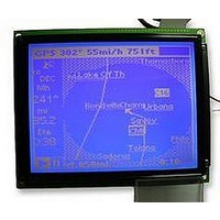
LMR4769EW-WCB
Manufacturer Part Number
LMR4769EW-WCB
Description
LCD MODULE, 240X320, BLUE
Manufacturer
DENSITRON
Datasheet
1.LMR4769EW-WCB.pdf
(108 pages)
Specifications of LMR4769EW-WCB
Lcd Display Type
STN
Pixel Size (h X W)
0.34mm X 0.34mm
Display Mode
Transflective
Interface Type
Serial
Viewing Area (h X W)
92.14mm X 120.14mm
Supply Voltage
32V
External Depth
15.6mm
External
RoHS Compliant
Svhc
No SVHC (15-Dec-2010)
Rohs Compliant
Yes
Backlighting Colour
Blue
Pixel Pitch (h X W)
0.36mm X 0.36mm


S1D13700 Technical Manual
CG RAM ADR
CSRDIR
CSRW
MWRITE
P1
P2
P1
P2
P1
P2
P3
P4
P5
P6
P7
P8
P9
P16
contiguous addresses in the display memory space. Therefore, the CG RAM addresses to which to
write data must be calculated as follows:
• Add addresses the same way as described above (M1 = 0).
• Change bit D6 in one character code from 1 to 0 when adding addresses.
Example of CG RAM definition (method of storing data) (See Figure 4-9 “Example of display
memory mapping” on page 63.)
Conditions
Setting list
• The pattern to define: Pattern A (8 x 16 dots per font) shown in Figure 4-1 “Character display
• Start address of the CG RAM table: 4800H
• Character code of defined pattern: 80H (first character code in CG RAM area)
([FX] 8 dots)” on page 45.
5CH
00H
40H
4CH
46H
00H
48H
70H
88H
88H
88H
F8H
88H
88H
00H
00H
00H
42H
Set SAG after calculating it by performing the method of CG RAM
address calculation in reverse.
Shift to the right
CG RAM area from 4800H
Write data for row 0
Write data for row 1
Write data for row 2
Write data for row 3
Write data for row 4
Write data for row 5
Write data for row 6
Write data for row 7
Write data for row 8
Write data for row 15
EPSON
4: FUNCTION DESCRIPTION
49
Related parts for LMR4769EW-WCB
Image
Part Number
Description
Manufacturer
Datasheet
Request
R

Part Number:
Description:
LCD MODULE, 128X240, YELLOW/GREEN
Manufacturer:
DENSITRON
Datasheet:

Part Number:
Description:
LCD MODULE, 128X240, BLUE
Manufacturer:
DENSITRON
Datasheet:

Part Number:
Description:
PMOLED, 128*128, COLOUR
Manufacturer:
DENSITRON
Datasheet:

Part Number:
Description:
DISPLAY, OLED, 128X32, BLUE
Manufacturer:
DENSITRON
Datasheet:
Part Number:
Description:
DISPLAY, OLED, 128X32, YLW
Manufacturer:
DENSITRON
Datasheet:
Part Number:
Description:
PMOLED, 128*64, WHITE
Manufacturer:
DENSITRON
Datasheet:
Part Number:
Description:
DISPLAY, OLED, 128X64, YELLOW
Manufacturer:
DENSITRON
Datasheet:

Part Number:
Description:
DISPLAY, OLED, 128X64, YELLOW
Manufacturer:
DENSITRON
Datasheet:
Part Number:
Description:
DISPLAY, OLED, 128X64, YELLOW
Manufacturer:
DENSITRON
Datasheet:
Part Number:
Description:
128 x 240 PIXEL INDUSTRIAL TOUCH MONITOR
Manufacturer:
Densitron Corporation
Part Number:
Description:
64 x 240 PIXEL INDUSTRIAL TOUCH MONITOR
Manufacturer:
Densitron Corporation
Part Number:
Description:
320 x 240 PIXEL INDUSTRIAL TOUCH MONITOR
Manufacturer:
Densitron Corporation
Part Number:
Description:
320 x 240 PIXEL INDUSTRIAL TOUCH MONITOR
Manufacturer:
Densitron Corporation
Part Number:
Description:
132 Seg / 65 Com Driver & Controller For Stn Lcd
Manufacturer:
Densitron Corporation
Datasheet: