LMR4769EW-WCB DENSITRON, LMR4769EW-WCB Datasheet - Page 95
LMR4769EW-WCB
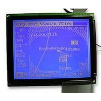
Manufacturer Part Number
LMR4769EW-WCB
Description
LCD MODULE, 240X320, BLUE
Manufacturer
DENSITRON
Datasheet
1.LMR4769EW-WCB.pdf
(108 pages)
Specifications of LMR4769EW-WCB
Lcd Display Type
STN
Pixel Size (h X W)
0.34mm X 0.34mm
Display Mode
Transflective
Interface Type
Serial
Viewing Area (h X W)
92.14mm X 120.14mm
Supply Voltage
32V
External Depth
15.6mm
External
RoHS Compliant
Svhc
No SVHC (15-Dec-2010)
Rohs Compliant
Yes
Backlighting Colour
Blue
Pixel Pitch (h X W)
0.36mm X 0.36mm


5: SPECIFICATIONS
90
Symbol
T
f
t10
t11
t12
t13
CLK
CLK
t1
t2
t3
t4
t5
t6
t7
t8
t9
BUS clock frequency
BUS clock period
AB [16 : 0], WR# (R/W#) and CS# and AS# and RD# (UDS#, LDS#)
setup to first CLK rising edge
CS# and AS# asserted to WAIT# (DTACK#) driven
RD# = 0 (UDS# = 0 or LDS# = 0) to DB [15 : 0] driven (read cycle)
AB [16 : 0], WR# (R/W#) and CS# hold from AS# rising edge
WAIT# (DTACK#) falling edge to RD# (UDS#, LDS#) rising edge
RD# (USD#, LDS#) deasserted high to reasserted low
CLK rising edge to WAIT# (DTACK#) high impedance
AS# rising edge to WAIT# (DTACK#) rising edge
DB [15 : 0] valid to 4th CLK rising edge where CS# = 0, AS# = 0 and
either RD# = 0 (UDS# = 0 or LDS# = 0) (wirte cycle)
DB [15 : 0] hold from RD# (UDS#, LDS#) falling edge (wirte cycle)
RD# (UDS#, LDS#) rising edge to DB [15 : 0] high impedance (read
cycle)
DB [15 : 0] valid setup time to 2nd CLK falling edge after WAIT#
(DTACK#) goes low (read cycle)
t13 Cycle Length
- When read
- when Write (next cycle = write cycle)
- when Write (next cycle = read cycle)
Read
Write (next write cycle)
Write (next read cycle)
Parameter
Motorola M68K#1 Interface Timing
EPSON
[V
SS
3Tclk+9ns
2Tclk+8ns
5Tclk+8ns
1/f
= 0V, V
1Tclk
Min.
—
—
11
1
0
1
3
4
9
1
6
6
7
8
CLK
DD
Spec
= 4.5 – 5.5V, Ta = -40 – 85°C]
S1D13700 Technical Manual
1T
Max.
CLK
—
—
—
—
64
—
—
—
12
—
—
—
—
7
-2
T
MHz
T
T
Unit
ns
ns
ns
ns
ns
ns
ns
ns
ns
ns
ns
ns
ns
CLK
CLK
CLK
Related parts for LMR4769EW-WCB
Image
Part Number
Description
Manufacturer
Datasheet
Request
R

Part Number:
Description:
LCD MODULE, 128X240, YELLOW/GREEN
Manufacturer:
DENSITRON
Datasheet:

Part Number:
Description:
LCD MODULE, 128X240, BLUE
Manufacturer:
DENSITRON
Datasheet:

Part Number:
Description:
PMOLED, 128*128, COLOUR
Manufacturer:
DENSITRON
Datasheet:

Part Number:
Description:
DISPLAY, OLED, 128X32, BLUE
Manufacturer:
DENSITRON
Datasheet:
Part Number:
Description:
DISPLAY, OLED, 128X32, YLW
Manufacturer:
DENSITRON
Datasheet:
Part Number:
Description:
PMOLED, 128*64, WHITE
Manufacturer:
DENSITRON
Datasheet:
Part Number:
Description:
DISPLAY, OLED, 128X64, YELLOW
Manufacturer:
DENSITRON
Datasheet:

Part Number:
Description:
DISPLAY, OLED, 128X64, YELLOW
Manufacturer:
DENSITRON
Datasheet:
Part Number:
Description:
DISPLAY, OLED, 128X64, YELLOW
Manufacturer:
DENSITRON
Datasheet:
Part Number:
Description:
128 x 240 PIXEL INDUSTRIAL TOUCH MONITOR
Manufacturer:
Densitron Corporation
Part Number:
Description:
64 x 240 PIXEL INDUSTRIAL TOUCH MONITOR
Manufacturer:
Densitron Corporation
Part Number:
Description:
320 x 240 PIXEL INDUSTRIAL TOUCH MONITOR
Manufacturer:
Densitron Corporation
Part Number:
Description:
320 x 240 PIXEL INDUSTRIAL TOUCH MONITOR
Manufacturer:
Densitron Corporation
Part Number:
Description:
132 Seg / 65 Com Driver & Controller For Stn Lcd
Manufacturer:
Densitron Corporation
Datasheet: