LMR4769EW-WCB DENSITRON, LMR4769EW-WCB Datasheet - Page 21
LMR4769EW-WCB
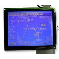
Manufacturer Part Number
LMR4769EW-WCB
Description
LCD MODULE, 240X320, BLUE
Manufacturer
DENSITRON
Datasheet
1.LMR4769EW-WCB.pdf
(108 pages)
Specifications of LMR4769EW-WCB
Lcd Display Type
STN
Pixel Size (h X W)
0.34mm X 0.34mm
Display Mode
Transflective
Interface Type
Serial
Viewing Area (h X W)
92.14mm X 120.14mm
Supply Voltage
32V
External Depth
15.6mm
External
RoHS Compliant
Svhc
No SVHC (15-Dec-2010)
Rohs Compliant
Yes
Backlighting Colour
Blue
Pixel Pitch (h X W)
0.36mm X 0.36mm


3: COMMANDS AND COMMAND REGISTERS
*1 To ensure that two bytes are set at the same time, the low-order byte is fixed when the high-order byte is written.
*2 SLEEPIN = 0: Clock enable
*3 CSRW: Write only (00h when read), CSRR: read only (write invalid).
The following shows the relationship between memory and register maps in the S1D13700.
16
0 x 8019
0 x 801A *
0 x 801B
0 x 801C *
0 x 801D *
0 x 801E *
0 x 801F *
0 x 8020
* The S1D13700 ignores any attempt to access address space 8030h–FFFFh. This address space may be employed as
Address
a user area, but because there is no negate output available for the WAIT# pin of the S1D13700, inhibit access to this
address space when not in use.
Other registers can be written to or read from (in units of bits).
3
3
3
1
3
0 x 00
0 x 00
0 x 00
0 x 00
0 x 00
0 x 00
0 x 00
0 x 00
Reset
Hard
Using the internal oscillator circuit causes the oscillator to start oscillating. Using an externally sourced
clock causes the clock to propagate to the internal circuits.
The internal timing circuit is released from reset status by writing to any register after setting SLEEPIN
= 0. (Therefore, internal SRAM cannot be accessed until that time.)
r_P1_
CGRAMAdr
r_P2_
CGRAMAdr
r_P1_HdotScr
r_P1_CSRW
r_P2_CSRW
r_P1_CSRR
r_P2_CSRR
r_P1_
GrayScale
Register name
FFFFh
7FFFh
85AFh
85B0h
802Fh
0000h
8000h
8030h
S1D13700 Memory Mapping (AB15 – AB0)
SAGH
SAGL
CSRH
CSRH
CSRL
CSRL
A15
A15
A15
bit7
A7
A7
A7
0
0
(MSB DB7 – LSB DB0)
0x8021 – 0x802F Reserve
SAGH
SAGL
CSRH
CSRH
CSRL
CSRL
(CGROM Area)
A14
A14
A14
bit6
A6
A6
A6
0
0
Register Area
Display RAM
Not Use
EPSON
Area
SAGL
SAGH
CSRH
CSRH
CSRL
CSRL
A13
A13
A13
bit5
A5
A5
A5
0
0
SAGH
SAGL
CSRH
CSRH
CSRL
CSRL
A12
A12
A12
bit4
A4
A4
A4
0
0
SAGH
SAGL
CSRH
CSRH
CSRL
CSRL
A11
A11
A11
bit3
A3
A3
A3
0
0
SAGH
SAGL
CSRH
CSRH
CSRL
CSRL
A10
A10
A10
bit2
A2
D2
A2
A2
0
S1D13700 Technical Manual
SAGH
SAGL
CSRH
CSRH
CSRL
CSRL
BPP1
bit1
A1
A9
D1
A1
A9
A1
A9
SAGH
SAGL
CSRH
CSRH
CSRL
CSRL
BPP0
bit0
D0
A0
A8
A0
A8
A0
A8
Related parts for LMR4769EW-WCB
Image
Part Number
Description
Manufacturer
Datasheet
Request
R

Part Number:
Description:
LCD MODULE, 128X240, YELLOW/GREEN
Manufacturer:
DENSITRON
Datasheet:

Part Number:
Description:
LCD MODULE, 128X240, BLUE
Manufacturer:
DENSITRON
Datasheet:

Part Number:
Description:
PMOLED, 128*128, COLOUR
Manufacturer:
DENSITRON
Datasheet:

Part Number:
Description:
DISPLAY, OLED, 128X32, BLUE
Manufacturer:
DENSITRON
Datasheet:
Part Number:
Description:
DISPLAY, OLED, 128X32, YLW
Manufacturer:
DENSITRON
Datasheet:
Part Number:
Description:
PMOLED, 128*64, WHITE
Manufacturer:
DENSITRON
Datasheet:
Part Number:
Description:
DISPLAY, OLED, 128X64, YELLOW
Manufacturer:
DENSITRON
Datasheet:

Part Number:
Description:
DISPLAY, OLED, 128X64, YELLOW
Manufacturer:
DENSITRON
Datasheet:
Part Number:
Description:
DISPLAY, OLED, 128X64, YELLOW
Manufacturer:
DENSITRON
Datasheet:
Part Number:
Description:
128 x 240 PIXEL INDUSTRIAL TOUCH MONITOR
Manufacturer:
Densitron Corporation
Part Number:
Description:
64 x 240 PIXEL INDUSTRIAL TOUCH MONITOR
Manufacturer:
Densitron Corporation
Part Number:
Description:
320 x 240 PIXEL INDUSTRIAL TOUCH MONITOR
Manufacturer:
Densitron Corporation
Part Number:
Description:
320 x 240 PIXEL INDUSTRIAL TOUCH MONITOR
Manufacturer:
Densitron Corporation
Part Number:
Description:
132 Seg / 65 Com Driver & Controller For Stn Lcd
Manufacturer:
Densitron Corporation
Datasheet: