MC33696MOD315EV Freescale Semiconductor, MC33696MOD315EV Datasheet - Page 10
MC33696MOD315EV
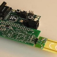
Manufacturer Part Number
MC33696MOD315EV
Description
MCU, MPU & DSP Development Tools MC33696 (ECHO) RF C EVAL
Manufacturer
Freescale Semiconductor
Datasheet
1.MC33696MOD868EV.pdf
(80 pages)
Specifications of MC33696MOD315EV
Processor To Be Evaluated
MC9S08RG60
Interface Type
RS-232
Lead Free Status / RoHS Status
Lead free / RoHS Compliant


MCU Interface
Table 5
10
•
•
•
•
•
STROBE — Wakeup control input
The STROBE pin controls the ON/OFF sequence of the MC33696. When STROBE is set to low
level, the receiver is off—when STROBE is set to high level, the receiver is on. The current
consumption in receive mode can be reduced by strobing the receiver. The periodic wakeup can be
done by MCU only or by an internal oscillator thanks to an external capacitor (strobe oscillator
must be previously enabled by setting SOE bit to 1). Refer to
Control,” for more details.
SEB — Serial interface enable control input
When SEB is set high, pins SCLK, MOSI, and MISO are set to high impedance, and the SPI bus
is disabled. When SEB is set low, SPI bus is enabled. This allows individual selection in a multiple
device system, where all devices are connected via the same bus. The rest of the circuit remains in
the current state, enabling fast recovery times, but the power amplifier is disabled to prevent any
uncontrolled RF transmission.
If the MCU shares the SPI access with the MC33696 only, SEB control by the MCU is optional.
If not used, it could be hardwired to 0.
SCLK — Serial clock input/output
Synchronizes data movement in and out of the device through its MOSI and MISO lines. The
master and slave devices can exchange a byte of information during a sequence of eight clock
cycles. Since SCLK is generated by the master device, this line is an input on the slave device.
MOSI — Master output slave input/output
In configuration mode, MOSI is an input.
In transmission mode, MOSI is an input and receives encoded data from MCU.
In receive mode, MOSI is an output. Received data is sent on MOSI (see
Transmits bytes when master, and receives bytes when slave, with the most significant bit first.
When no data are output, SCLK and MOSI force a low level.
MISO — Master input/slave output
In configuration mode only, data read from registers is sent to the MCU with the MSB first. There
is no master function. Data are valid on falling edges of SCLK. This means that the clock phase
and polarity control bits of the microcontroller SPI have to be CPOL = 0 and CPHA = 1 (using
Freescale acronyms).
Configuration
Transmit
Receive
Standby / LVD
summarizes the serial digital interface feature versus the selected mode.
Selected Mode
DME = 1
DME = 0
Table 5. Serial Digital Interface Feature versus Selected Mode
SPI slave, data received on MOSI, SCLK from MCU, MISO is output (SEB=0)
SPI deselected, MOSI receives encoded data from MCU (SEB =0)
SPI master, data sent on MOSI with clock on SCLK (SEB=0)
SPI deselected, received data are directly sent to MOSI (SEB=0)
SPI deselected, all I/O are high impedance (SEB =1)
MC33696 Data Sheet, Rev. 12
MC33696 Digital Interface Use
Section 12.3, “Receiver On/Off
Table
Freescale Semiconductor
5).
Related parts for MC33696MOD315EV
Image
Part Number
Description
Manufacturer
Datasheet
Request
R

Part Number:
Description:
Manufacturer:
Freescale Semiconductor, Inc
Datasheet:
Part Number:
Description:
Manufacturer:
Freescale Semiconductor, Inc
Datasheet:
Part Number:
Description:
Manufacturer:
Freescale Semiconductor, Inc
Datasheet:
Part Number:
Description:
Manufacturer:
Freescale Semiconductor, Inc
Datasheet:
Part Number:
Description:
Manufacturer:
Freescale Semiconductor, Inc
Datasheet:
Part Number:
Description:
Manufacturer:
Freescale Semiconductor, Inc
Datasheet:
Part Number:
Description:
Manufacturer:
Freescale Semiconductor, Inc
Datasheet:
Part Number:
Description:
Manufacturer:
Freescale Semiconductor, Inc
Datasheet:
Part Number:
Description:
Manufacturer:
Freescale Semiconductor, Inc
Datasheet:
Part Number:
Description:
Manufacturer:
Freescale Semiconductor, Inc
Datasheet:
Part Number:
Description:
Manufacturer:
Freescale Semiconductor, Inc
Datasheet:
Part Number:
Description:
Manufacturer:
Freescale Semiconductor, Inc
Datasheet:
Part Number:
Description:
Manufacturer:
Freescale Semiconductor, Inc
Datasheet:
Part Number:
Description:
Manufacturer:
Freescale Semiconductor, Inc
Datasheet:
Part Number:
Description:
Manufacturer:
Freescale Semiconductor, Inc
Datasheet: