MC33696MOD315EV Freescale Semiconductor, MC33696MOD315EV Datasheet - Page 73
MC33696MOD315EV
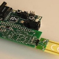
Manufacturer Part Number
MC33696MOD315EV
Description
MCU, MPU & DSP Development Tools MC33696 (ECHO) RF C EVAL
Manufacturer
Freescale Semiconductor
Datasheet
1.MC33696MOD868EV.pdf
(80 pages)
Specifications of MC33696MOD315EV
Processor To Be Evaluated
MC9S08RG60
Interface Type
RS-232
Lead Free Status / RoHS Status
Lead free / RoHS Compliant


23
Pay attention to the following points and recommendations when designing the layout of the PCB.
Freescale Semiconductor
•
•
•
Ground Plane
— If you can afford a multilayer PCB, use an internal layer for the ground plane, route power
— Use at least a double-sided PCB.
— Use a large ground plane on the opposite layer.
— If the ground plane must be cut on the opposite layer for routing some signals, maintain
Power Supply, Ground Connection and Decoupling
— Connect each ground pin to the ground plane using a separate via for each signal; do not use
— Place each decoupling capacitor as close to the corresponding VCC pin as possible (no more
— Locate the VCCDIG2 decoupling capacitor (C10) directly between VCCDIG2 (pin 14) and
— GNDPA1 and GNDPA2 inductance to ground should be minimum. If possible, use two via for
RF Tracks, Matching Network and Other Components
— Minimize any tracks used for routing RF signals.
— Locate crystal X1 and associated capacitors C6 and C7 close to the MC33696. Avoid loops
— Use high frequency coils with high Q values for the frequency of operation (minimum of 15).
— Track between RFOUT and RFIN should be as short as possible to minimize lost in TX mode.
PCB Design Recommendations
supply and digital signals on the last layer, with RF components on the first layer.
continuity with another ground plane on the opposite layer and a lot of via to minimize
parasitic inductance.
common vias.
than 2–3 mm away).
GND (pin 16).
each pin.
occurring due to component size and tracks. Avoid routing digital signals in this area.
Validate any change of coil source.
The values indicated for the matching network have been computed and
tuned for the MC33696 RF Modules available for MC33696 evaluation.
Matching networks should be retuned if any change is made to the PCB
(track width, length or place, or PCB thickness, or component value). Never
use, as is, a matching network designed for another PCB.
MC33696 Data Sheet, Rev. 12
NOTE
PCB Design Recommendations
73
Related parts for MC33696MOD315EV
Image
Part Number
Description
Manufacturer
Datasheet
Request
R

Part Number:
Description:
Manufacturer:
Freescale Semiconductor, Inc
Datasheet:
Part Number:
Description:
Manufacturer:
Freescale Semiconductor, Inc
Datasheet:
Part Number:
Description:
Manufacturer:
Freescale Semiconductor, Inc
Datasheet:
Part Number:
Description:
Manufacturer:
Freescale Semiconductor, Inc
Datasheet:
Part Number:
Description:
Manufacturer:
Freescale Semiconductor, Inc
Datasheet:
Part Number:
Description:
Manufacturer:
Freescale Semiconductor, Inc
Datasheet:
Part Number:
Description:
Manufacturer:
Freescale Semiconductor, Inc
Datasheet:
Part Number:
Description:
Manufacturer:
Freescale Semiconductor, Inc
Datasheet:
Part Number:
Description:
Manufacturer:
Freescale Semiconductor, Inc
Datasheet:
Part Number:
Description:
Manufacturer:
Freescale Semiconductor, Inc
Datasheet:
Part Number:
Description:
Manufacturer:
Freescale Semiconductor, Inc
Datasheet:
Part Number:
Description:
Manufacturer:
Freescale Semiconductor, Inc
Datasheet:
Part Number:
Description:
Manufacturer:
Freescale Semiconductor, Inc
Datasheet:
Part Number:
Description:
Manufacturer:
Freescale Semiconductor, Inc
Datasheet:
Part Number:
Description:
Manufacturer:
Freescale Semiconductor, Inc
Datasheet: