MC33696MOD315EV Freescale Semiconductor, MC33696MOD315EV Datasheet - Page 6
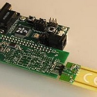
MC33696MOD315EV
Manufacturer Part Number
MC33696MOD315EV
Description
MCU, MPU & DSP Development Tools MC33696 (ECHO) RF C EVAL
Manufacturer
Freescale Semiconductor
Datasheet
1.MC33696MOD868EV.pdf
(80 pages)
Specifications of MC33696MOD315EV
Processor To Be Evaluated
MC9S08RG60
Interface Type
RS-232
Lead Free Status / RoHS Status
Lead free / RoHS Compliant


NOTES:
1
Power Supply
5
The circuit can be supplied from a 3 V voltage regulator or battery cell by connecting VCCIN,
VCCINOUT, and VCCDIG (See
connected to VCCIN; in this case VCCINOUT and VCCDIG should not be connected to VCCIN (See
Figure 45
The RFOUT pin cannot be biased with a voltage higher than 3.6 V. For 5 V operation, biasing voltage is
available on VCCINOUT.
An on-chip low drop-out voltage regulator supplies the RF and analog modules (except the strobe
oscillator and the low voltage detector, which are directly supplied from VCCINOUT). This voltage
regulator is supplied from pin VCCINOUT and its output is connected to VCC2OUT. An external
capacitor (C8 = 100 nF) must be inserted between VCC2OUT and GND for stabilization and decoupling.
The analog and RF modules must be supplied by VCC2 by externally wiring VCC2OUT to VCC2IN,
VCC2RF, and VCC2VCO.
A second voltage regulator supplies the digital part. This regulator is powered from pin VCCDIG and its
output is connected to VCCDIG2. An external capacitor (C10 = 100 nF) must be inserted between
VCCDIG2 and GNDDIG, for decoupling. The supply voltage VCCDIG2 is equal to 1.6 V. In standby
mode, this voltage regulator goes into an ultra-low-power mode, but VCCDIG2 = 0.7 × V
This enables the internal registers to be supplied, allowing configuration data to be saved.
6
At power-on, an internal reset signal (Power-on Reset, POR) is generated when supply voltage is around
1.3 V. All registers are reset.
When the LVDE bit is set, the low-voltage detection module is enabled. This block compares the supply
voltage on VCCINOUT with a reference level of about 1.8 V. If the voltage on VCCINOUT drops below
1.8 V, status bit LVDS is set. The information in status bit LVDS is latched and reset after a read access.
6
Supply voltage on VCCIN, VCCINOUT, VCCDIG for 3 V operation
Supply voltage on VCCIN for 5 V operation
Supply voltage on VCCPA for 3 V or 5 V operation
–40°C to +85°C: MC33696FCE/FJE.
–20°C to +85°C: MC33696FCAE/FJAE.
Power Supply
Supply Voltage Monitoring and Reset
or
Figure
46).
Table 3. Supply Voltage Range Versus Ambient Temperature
Parameter
Figure 43
MC33696 Data Sheet, Rev. 12
or
Figure
44). It is also possible to use a 5 V power supply
Symbol
V
V
V
CC3V
CC5V
CCPA
–40°C to +85°C
2.7 to 3.6
4.5 to 5.5
3.0 to 3.6
Temperature Range
–20°C to +85°C
Freescale Semiconductor
2.1 to 3.6
4.5 to 5.5
3.0 to 3.6
CCDIG.
1
Unit
V
V
V
Related parts for MC33696MOD315EV
Image
Part Number
Description
Manufacturer
Datasheet
Request
R

Part Number:
Description:
Manufacturer:
Freescale Semiconductor, Inc
Datasheet:
Part Number:
Description:
Manufacturer:
Freescale Semiconductor, Inc
Datasheet:
Part Number:
Description:
Manufacturer:
Freescale Semiconductor, Inc
Datasheet:
Part Number:
Description:
Manufacturer:
Freescale Semiconductor, Inc
Datasheet:
Part Number:
Description:
Manufacturer:
Freescale Semiconductor, Inc
Datasheet:
Part Number:
Description:
Manufacturer:
Freescale Semiconductor, Inc
Datasheet:
Part Number:
Description:
Manufacturer:
Freescale Semiconductor, Inc
Datasheet:
Part Number:
Description:
Manufacturer:
Freescale Semiconductor, Inc
Datasheet:
Part Number:
Description:
Manufacturer:
Freescale Semiconductor, Inc
Datasheet:
Part Number:
Description:
Manufacturer:
Freescale Semiconductor, Inc
Datasheet:
Part Number:
Description:
Manufacturer:
Freescale Semiconductor, Inc
Datasheet:
Part Number:
Description:
Manufacturer:
Freescale Semiconductor, Inc
Datasheet:
Part Number:
Description:
Manufacturer:
Freescale Semiconductor, Inc
Datasheet:
Part Number:
Description:
Manufacturer:
Freescale Semiconductor, Inc
Datasheet:
Part Number:
Description:
Manufacturer:
Freescale Semiconductor, Inc
Datasheet: