MC33696MOD315EV Freescale Semiconductor, MC33696MOD315EV Datasheet - Page 35
MC33696MOD315EV
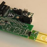
Manufacturer Part Number
MC33696MOD315EV
Description
MCU, MPU & DSP Development Tools MC33696 (ECHO) RF C EVAL
Manufacturer
Freescale Semiconductor
Datasheet
1.MC33696MOD868EV.pdf
(80 pages)
Specifications of MC33696MOD315EV
Processor To Be Evaluated
MC9S08RG60
Interface Type
RS-232
Lead Free Status / RoHS Status
Lead free / RoHS Compliant


17.1.3.1 BANKA = X, BANKB = 0
If strobe pin is 1, configuration is defined by Bank A, BANKS = 1.
If strobe pin is 0, MC33696 configuration is OFF.
If a message is received during State A, current state remains State A up to end of message.
17.1.3.2 BANKA = 0, BANKB = 1
If strobe pin is 1, configuration is defined by Bank B, BANKS = 0.
If strobe pin is 0, MC33696 configuration is OFF.
If a message is received during State B, current state remains State B up to end of message.
17.1.3.3 BANKA = 1, BANK B = 1
BANKS toggles at the end of each state A or state B.
If strobe is forced to 1, configuration is frozen according to BANKS value.
If a read or write access is done using SPI, the next sequence will begin with state A in whatever was the
active state before SPI access by MCU.
For all available sequences:
Freescale Semiconductor
Strobe
Banks
Banks Bit
State A
State A
A
•
•
•
•
•
•
State B
1
Z
State A and State B are defined by Bank A and Bank B.
State A duration, TonA is defined by Bank A RON[3–0].
State B duration, TonB is defined by Bank B RON[3–0].
OFF duration, TonB is defined by Bank A ROFF[2–0].
If strobe pin is 1, the state is ON and defined by BANKS at that time. It remains this state up to
the release of strobe and end of message if a message is being received.
If a message is being received during State A or B, current state remains State A or B up to end of
message.
B
State B
OFF
OFF
OFF
A
B
OFF
State A
MC33696 Data Sheet, Rev. 12
OFF
State B
StateA
A
OFF
StateB
B
OFF
OFF
State A
Configuration Switching
State B
A
OFF
B
35
Related parts for MC33696MOD315EV
Image
Part Number
Description
Manufacturer
Datasheet
Request
R

Part Number:
Description:
Manufacturer:
Freescale Semiconductor, Inc
Datasheet:
Part Number:
Description:
Manufacturer:
Freescale Semiconductor, Inc
Datasheet:
Part Number:
Description:
Manufacturer:
Freescale Semiconductor, Inc
Datasheet:
Part Number:
Description:
Manufacturer:
Freescale Semiconductor, Inc
Datasheet:
Part Number:
Description:
Manufacturer:
Freescale Semiconductor, Inc
Datasheet:
Part Number:
Description:
Manufacturer:
Freescale Semiconductor, Inc
Datasheet:
Part Number:
Description:
Manufacturer:
Freescale Semiconductor, Inc
Datasheet:
Part Number:
Description:
Manufacturer:
Freescale Semiconductor, Inc
Datasheet:
Part Number:
Description:
Manufacturer:
Freescale Semiconductor, Inc
Datasheet:
Part Number:
Description:
Manufacturer:
Freescale Semiconductor, Inc
Datasheet:
Part Number:
Description:
Manufacturer:
Freescale Semiconductor, Inc
Datasheet:
Part Number:
Description:
Manufacturer:
Freescale Semiconductor, Inc
Datasheet:
Part Number:
Description:
Manufacturer:
Freescale Semiconductor, Inc
Datasheet:
Part Number:
Description:
Manufacturer:
Freescale Semiconductor, Inc
Datasheet:
Part Number:
Description:
Manufacturer:
Freescale Semiconductor, Inc
Datasheet: