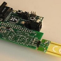
MC33696MOD315EV Freescale Semiconductor, MC33696MOD315EV Datasheet - Page 31

MC33696MOD315EV
Manufacturer Part Number
MC33696MOD315EV
Description
MCU, MPU & DSP Development Tools MC33696 (ECHO) RF C EVAL
Manufacturer
Freescale Semiconductor
Datasheet
1.MC33696MOD868EV.pdf
(80 pages)
Specifications of MC33696MOD315EV
Processor To Be Evaluated
MC9S08RG60
Interface Type
RS-232
Lead Free Status / RoHS Status
Lead free / RoHS Compliant
17
This feature allows for defining two different configurations using two different banks, and for switching
them automatically during wakeup when using a strobe oscillator, or by means of the strobe pin actuation
by the MCU. This automatic feature may be used only in receiver mode; however, if one of the register
banks is related to a transmitter configuration, it may be accessed directly by programing some bits to
define the active bank, thus allowing fast switching between receiver mode and transmitter mode, or
between any different possible configurations.
Freescale Semiconductor
(Section 10)
*Refer to
2. A high level is applied on STROBE in order to wake the MC33696 and enter transmit/receive
3. CONFB and SEB must be forced to low level to enter configuration mode. Register values are
Proposed solutions to verify these conditions are :
— If the receiver does not wake periodically and it is only controlled by the STROBE pin (strobe
— If the receiver wakes periodically (strobe oscillator enable SOE = 1), the state of the MCU
mode. The duration of this state should be greater than the sum of lock time parameter 5.9 and
5.10. Refer to
writen into the internal registers of the MC33696. Refer to
and to
STROBE
STROBE
CONFB
CONFB
VCC
VCC
SCLK
SCLK
MOSI
MOSI
MISO
MISO
Configuration Switching
SEB
SEB
oscillator disable SOE = 0), an external pulldown resistor on STROBE is required (see
Figure 43
pins must be defined first and then a power supply must be applied to the MC33696. A
transistor can be used to control the power supply on the VCCIN pin of the MC33696. This
transistor will be driven by an MCU I/O (see
strobe oscillator mode).
1
1
0
0
1
1
0
0
1
1
0
0
1
1
0
0
1
1
0
0
1
1
0
0
Figure
3V
3V
0
0
1
1
45.
for a 3 V application schematic).
Section 15, “Configuration
2
2
N1N0 A4 A3 A2 A1 A0 R/W
N1N0 A4 A3 A2 A1 A0 R/W
Figure 24. Startup sequence
MC33696 Data Sheet, Rev. 12
Mode.”
Figure 44
D7 D6 D5 D4 D3 D2 D1 D0
D7 D6 D5 D4 D3 D2 D1 D0
3
3
Section 15, “Configuration
for a 3 V application schematic in
Configuration Switching
D7 D6 D5 D4 D3 D2 D1 D0
D7 D6 D5 D4 D3 D2 D1 D0
Mode,”
31


