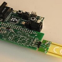
MC33696MOD315EV Freescale Semiconductor, MC33696MOD315EV Datasheet - Page 41

MC33696MOD315EV
Manufacturer Part Number
MC33696MOD315EV
Description
MCU, MPU & DSP Development Tools MC33696 (ECHO) RF C EVAL
Manufacturer
Freescale Semiconductor
Datasheet
1.MC33696MOD868EV.pdf
(80 pages)
Specifications of MC33696MOD315EV
Processor To Be Evaluated
MC9S08RG60
Interface Type
RS-232
Lead Free Status / RoHS Status
Lead free / RoHS Compliant
- Current page: 41 of 80
- Download datasheet (2Mb)
A first SPI access allows RAGC to be set; a second SPI access is required to reset it.
FAGC (Freeze Automatic Gain Control) freezes both receiver AGC levels.
BANKS indicates which register bank is active. This bit, available in Bank A and Bank B, returns the same
value.
18.3 Frequency Registers
Figure 29
Freescale Semiconductor
Reset Value
Reset Value
Reset Value
Reset Value
Reset Value
Bit Name
Bit Name
Bit Name
Bit Name
Bit Name
Access
Access
Access
Access
Access
1 = Sets the gain to its maximum value
0 = No action
1= Holds the gain at its current value
0 = Bank B
1 = Bank A
and
Figure 30
FTA11
Bit 15
FSK3
Bit 23
Bit 15
FTB7
FTA3
Bit 7
Bit 7
R/W
R/W
R/W
R/W
R/W
F7
0
0
0
0
0
define the Frequency registers, F and FT.
FTA10
Bit 14
Bit 22
Bit 14
FSK2
FTB6
FTA2
Bit 6
Bit 6
R/W
R/W
R/W
R/W
R/W
F6
1
0
1
0
0
Bit 13
Bit 21
Bit 13
FSK1
FTB5
FTA9
FTA1
Bit 5
Bit 5
R/W
R/W
R/W
R/W
R/W
F5
0
0
1
0
0
MC33696 Data Sheet, Rev. 12
Figure 30. FT Register
Figure 29. F Register
Bit 12
Bit 20
Bit 12
FSK0
FTB4
FTA8
FTA0
Bit 4
Bit 4
R/W
R/W
R/W
R/W
R/W
F4
0
0
1
0
0
FTB11
Bit 11
Bit 19
Bit 11
FTB3
FTA7
Bit 3
Bit 3
R/W
R/W
R/W
R/W
R/W
F11
F3
1
0
0
0
0
FTB10
Bit 10
Bit 18
Bit 10
FTB2
FTA6
R/W
Bit 2
R/W
R/W
R/W
Bit 2
R/W
F10
F2
0
0
0
1
0
Bit 17
FTB9
FTB1
FTA5
Bit 9
R/W
Bit 1
R/W
R/W
Bit 9
R/W
Bit 1
R/W
F9
F1
0
0
0
1
0
Register Description
Bit 16
FTB8
FTB0
FTA4
Bit 8
R/W
Bit 0
R/W
R/W
Bit 8
R/W
Bit 0
R/W
F8
F0
0
0
0
1
1
Addr
Addr
$04
$05
$06
$07
$08
41
Related parts for MC33696MOD315EV
Image
Part Number
Description
Manufacturer
Datasheet
Request
R
Part Number:
Description:
Manufacturer:
Freescale Semiconductor, Inc
Datasheet:
Part Number:
Description:
Manufacturer:
Freescale Semiconductor, Inc
Datasheet:
Part Number:
Description:
Manufacturer:
Freescale Semiconductor, Inc
Datasheet:
Part Number:
Description:
Manufacturer:
Freescale Semiconductor, Inc
Datasheet:
Part Number:
Description:
Manufacturer:
Freescale Semiconductor, Inc
Datasheet:
Part Number:
Description:
Manufacturer:
Freescale Semiconductor, Inc
Datasheet:
Part Number:
Description:
Manufacturer:
Freescale Semiconductor, Inc
Datasheet:
Part Number:
Description:
Manufacturer:
Freescale Semiconductor, Inc
Datasheet:
Part Number:
Description:
Manufacturer:
Freescale Semiconductor, Inc
Datasheet:
Part Number:
Description:
Manufacturer:
Freescale Semiconductor, Inc
Datasheet:
Part Number:
Description:
Manufacturer:
Freescale Semiconductor, Inc
Datasheet:
Part Number:
Description:
Manufacturer:
Freescale Semiconductor, Inc
Datasheet:
Part Number:
Description:
Manufacturer:
Freescale Semiconductor, Inc
Datasheet:
Part Number:
Description:
Manufacturer:
Freescale Semiconductor, Inc
Datasheet:
Part Number:
Description:
Manufacturer:
Freescale Semiconductor, Inc
Datasheet:


