MC33696MOD315EV Freescale Semiconductor, MC33696MOD315EV Datasheet - Page 27
MC33696MOD315EV
Manufacturer Part Number
MC33696MOD315EV
Description
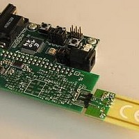
MCU, MPU & DSP Development Tools MC33696 (ECHO) RF C EVAL
Manufacturer
Freescale Semiconductor
Datasheet
1.MC33696MOD868EV.pdf
(80 pages)
Specifications of MC33696MOD315EV
Processor To Be Evaluated
MC9S08RG60
Interface Type
RS-232
Lead Free Status / RoHS Status
Lead free / RoHS Compliant


See the FRM bit description
setting carrier frequencies.
See
13.2 State Machine
In transmit mode, the state diagram is reduced to only one state: state 30. The circuit is either waiting for
a digital telegram to send, or is sending one. In this mode, the circuit can be considered as a simple RF
physical interface. The information presented on MOSI is sent directly in RF (according to the selected
modulation), with no internal processing.
Data transmission is possible only if the PLL is within the lock-in range. Therefore, during transmission,
if the PLL switches out of lock-in range, the RF output stage is switched off internally, thereby preventing
data from being transmitted in an unwanted band.
14
The SPI is deselected. CONFB is set to high level and STROBE to low level in order to enter this mode.
Nothing is sent and all incoming data are ignored until CONFB and SEB go low to switch back to
configuration mode.
Standby/LVD mode allows minimum current consumption to be achieved. Depending upon the value of
the LVDE bit, the circuit is in standby mode (state 60) or LVD mode (state 5 and 20).
LVDE = 0: The transceiver is in standby; consumption is reduced to leakage current (current state after
POR).
LVDE = 1: The LVD function is enabled; consumption is in the range of tens of microamperes.
The only way to exit this mode is to go back to configuration mode by applying a low level to CONFB and
a high level to STROBE.
15
15.1 Description
This mode is used to write or read the internal registers of the MC33696.
As long as a low level is applied to CONFB and a high level to STROBE (see
master node driving the SCLK input, the MOSI line input, and the MISO line output. Whatever the
direction, SPI transfers are 8-bit based and always begin with a command byte, which is supplied by the
MCU on MOSI. To be considered as a command byte, this byte must come after a falling edge on CONFB.
Figure 19
Freescale Semiconductor
Section 10, “MCU
Standby: LVD Mode
Configuration Mode
shows the content of the command byte.
Interface,” for more details about setting the level on the SEB pin.
(Figure
26) and
MC33696 Data Sheet, Rev. 12
Section 18.3, “Frequency
Registers,” for more details about
Figure
2), the MCU is the
Standby: LVD Mode
27
Related parts for MC33696MOD315EV
Image
Part Number
Description
Manufacturer
Datasheet
Request
R

Part Number:
Description:
Manufacturer:
Freescale Semiconductor, Inc
Datasheet:
Part Number:
Description:
Manufacturer:
Freescale Semiconductor, Inc
Datasheet:
Part Number:
Description:
Manufacturer:
Freescale Semiconductor, Inc
Datasheet:
Part Number:
Description:
Manufacturer:
Freescale Semiconductor, Inc
Datasheet:
Part Number:
Description:
Manufacturer:
Freescale Semiconductor, Inc
Datasheet:
Part Number:
Description:
Manufacturer:
Freescale Semiconductor, Inc
Datasheet:
Part Number:
Description:
Manufacturer:
Freescale Semiconductor, Inc
Datasheet:
Part Number:
Description:
Manufacturer:
Freescale Semiconductor, Inc
Datasheet:
Part Number:
Description:
Manufacturer:
Freescale Semiconductor, Inc
Datasheet:
Part Number:
Description:
Manufacturer:
Freescale Semiconductor, Inc
Datasheet:
Part Number:
Description:
Manufacturer:
Freescale Semiconductor, Inc
Datasheet:
Part Number:
Description:
Manufacturer:
Freescale Semiconductor, Inc
Datasheet:
Part Number:
Description:
Manufacturer:
Freescale Semiconductor, Inc
Datasheet:
Part Number:
Description:
Manufacturer:
Freescale Semiconductor, Inc
Datasheet:
Part Number:
Description:
Manufacturer:
Freescale Semiconductor, Inc
Datasheet: