MC33696MOD434EV Freescale Semiconductor, MC33696MOD434EV Datasheet - Page 11
MC33696MOD434EV
Manufacturer Part Number
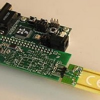
MC33696MOD434EV
Description
MCU, MPU & DSP Development Tools MC33696 (ECHO) RF C EVAL
Manufacturer
Freescale Semiconductor
Specifications of MC33696MOD434EV
Processor To Be Evaluated
MC9S08RG60
Interface Type
RS-232
Lead Free Status / RoHS Status
Lead free / RoHS Compliant


The data transfer protocol for each mode is described in the following sections.
11.2 Configuration Mode
This mode is used to write or read the internal registers of the MC33696.
As long as a low level is applied to CONFB (see
input, the MOSI line input, and the MISO line output. Whatever the direction, SPI transfers are 8-bit based
and always begin with a command byte, which is supplied by the MCU on MOSI. To be considered as a
command byte, this byte must come after a falling edge on CONFB.
command byte.
Bits N[1:0] specify the number of accessed registers, as defined in
Bits A[4:0] specify the address of the first register to access. This address is then incremented internally
by N after each data byte transfer.
R/W specifies the type of operation:
Thus, this bit is associated with the presence of information on MOSI (when writing) or MISO (when
reading).
Freescale Semiconductor
Bit Name
0 = Read
1 = Write
Configuration
Transmit
Receive
Standby / LVD
Selected Mode
Table 5. Serial Digital Interface Feature versus Selected Mode (SEB = 1)
DME = 1
DME = 0
Bit 7
N1
SPI slave, data received on MOSI, SCLK from MCU, MISO is output
SPI deselected, MOSI receives encoded data from MCU
SPI master, data sent on MOSI with clock on SCLK
SPI deselected, received data are directly sent to MOSI
SPI deselected, all I/O are high impedance
Bit 6
N0
N[1:0]
Table 6. Number N of Accessed Registers
00
01
10
11
Bit 5
Figure 3. Command Byte
MC33696 Data Sheet, Rev. 9
A4
Number N of Accessed Registers
Figure
MC33696 Digital Interface Use
Bit 4
A3
29), the MCU is the master node driving the SCLK
1
2
4
8
Bit 3
A2
Table
Figure 3
Bit 2
A1
6.
shows the content of the
Register Access through SPI
Bit 1
A0
Bit 0
R/W
11
Related parts for MC33696MOD434EV
Image
Part Number
Description
Manufacturer
Datasheet
Request
R

Part Number:
Description:
Manufacturer:
Freescale Semiconductor, Inc
Datasheet:
Part Number:
Description:
Manufacturer:
Freescale Semiconductor, Inc
Datasheet:
Part Number:
Description:
Manufacturer:
Freescale Semiconductor, Inc
Datasheet:
Part Number:
Description:
Manufacturer:
Freescale Semiconductor, Inc
Datasheet:
Part Number:
Description:
Manufacturer:
Freescale Semiconductor, Inc
Datasheet:
Part Number:
Description:
Manufacturer:
Freescale Semiconductor, Inc
Datasheet:
Part Number:
Description:
Manufacturer:
Freescale Semiconductor, Inc
Datasheet:
Part Number:
Description:
Manufacturer:
Freescale Semiconductor, Inc
Datasheet:
Part Number:
Description:
Manufacturer:
Freescale Semiconductor, Inc
Datasheet:
Part Number:
Description:
Manufacturer:
Freescale Semiconductor, Inc
Datasheet:
Part Number:
Description:
Manufacturer:
Freescale Semiconductor, Inc
Datasheet:
Part Number:
Description:
Manufacturer:
Freescale Semiconductor, Inc
Datasheet:
Part Number:
Description:
Manufacturer:
Freescale Semiconductor, Inc
Datasheet:
Part Number:
Description:
Manufacturer:
Freescale Semiconductor, Inc
Datasheet:
Part Number:
Description:
Manufacturer:
Freescale Semiconductor, Inc
Datasheet: